Welcome to the MCP3008 10-bit Analog-to-Digital Converter (ADC) from Microchip. This module will cover the functionality of the chip based on the datasheet.
Objectives
- Understand the various operating characteristics of the MCP3008.
- Understand the difference between single channel vs. differential pair input.
- Understand how VREF is used.
- Calculate the bit value for a 5V reference and a 3.3V (3V3) volt reference.
- Understand the timing technique required to allow a voltage sample to be taken.
Background
SPI Signals
How To Read A Datasheet
Microchip MCP3008 Datasheet
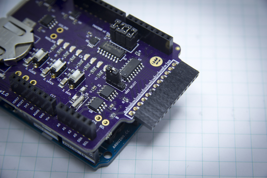
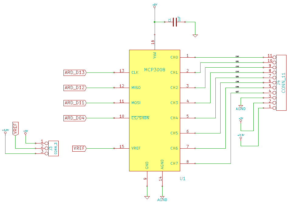
Schematic
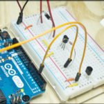
Education Shield – MCP3800 ADC Subsystem
Setup
There is no setup required for this module.
MCP3008 Functionality Overview
The Microchip MCP3008 is an eight channel, 10-bit ADC. At it’s most basic, it works just like the Analog Input pins do on the Arduino with the same level of resolution. The interface to send and receive data from the MCP3008 is SPI, so we’ll be using all the information in the SPI Basics modules to work with this chip.
Eight Channels
The “eight channels” refers to the fact that the MCP3008 is able to receive and process voltages on eight different inputs, number 0-7. These channels can be read in two different ways. The typical fashion is called “single ended input”, where the voltage level is read between the selected voltage reference, VREF, easily selected on the I2C and SPI Education Shield using the VREF jumper, and a ground level shared in common with the circuit doing the measuring and the circuit being measured. This is the method of measurement that most everyone is familiar with. The other capability is to read a differential input between a pair of pins, IN+ and IN-. With the differential input, you can read the voltage difference between the two inputs, and even use them to clean up a little bit of signal noise.
10 Bits
The 10 bits refers to the sampling range of the ADC itself. B0000000000 = 0 and B1111111111 = 1023, meaning you can measure 1024 different voltage levels, typically between ground and VREF. So if you have a 5V reference, and can split it 1024 times, each step would be equivalent to a measurement of 0.0049V. With the 3V3 reference, each step is equivalent to a measurement of 0.0032V. Smaller voltage references can be used as well, especially in conjunction with the differential input feature, to generate even smaller voltage values per step, but eventually you reach a point where you begin to introduce errors in your measurement.
VREF and AGND
VREF stands for “voltage reference” and it is the voltage we measure against as a standard to say “how much more or less than this is the signal we’re testing.” The Education Shield conveniently provides 5V and 3V3 reference with a jumper to select them (in later modules I’ll show how you can bring your own voltage reference in as well).
With a single ended measurement, you are measuring the signal level between the VREF you select and AGND. AGND stands for “Analog Ground” and for the purposes of the I2C and SPI Education Shield, it sits at the same potential as GND for the rest of the board. However, the actual physical copper that connects the AGND pin of the MCP3008 back to the GND connection on the Arduino through the PCB, is isolated from the rest of the ground plane on the board and was intentionally routed away from all serial signals to minimize the effect of coupling noise. If you’re performing a single ended measurement, always make sure that you use the AGND connection on the ADC header to ensure that the signal your referencing shares a common ground with the ADC itself.
MCP3008 Timing Specifics
The timing of your data transmission with respect to the ADC is somewhat crucial, in that you have to account for the chip needing a brief moment to actually perform a measurement of the type you desire, before you attempt to read it. The general sequence runs like this:
- Tell the chip to get ready to perform a measurement.
- Tell the chip which single channel or differential pair to measure.
- Give the chip time to perform the measurement.
- Begin reading back the data of the measurement.
Of course, since this is all SPI, we also need to wrap that entire sequence inside taking the ADC CS low, running the sequence, then bringing the ADC CS high again.
Get Ready
According to the MCP3008 datasheet, the first bit received after the CS pin goes low is the start bit. This will tell the ADC that it needs to be ready to perform a measurement.
Get Set
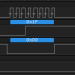
Immediately after the start bit is received, the next immediate bit will tell the MCP3008 if you intend to perform a single or a differential measurement, 1 = single, 0 = differential. This is followed by three bits determining which channel or channels will be used for the measurement. These bits must be sent immediately after the start bit, so care must be taken to ensure that data is clocked out on MOSI in this order.
| SINGLE/DIFF | BIT2 | BIT1 | BIT0 | CONFIGURATION | CHANNEL |
|---|---|---|---|---|---|
| 1 | 0 | 0 | 0 | SINGLE | CH0 |
| 1 | 0 | 0 | 1 | SINGLE | CH1 |
| 1 | 0 | 1 | 0 | SINGLE | CH2 |
| 1 | 0 | 1 | 1 | SINGLE | CH3 |
| 1 | 1 | 0 | 0 | SINGLE | CH4 |
| 1 | 1 | 0 | 1 | SINGLE | CH5 |
| 1 | 1 | 1 | 0 | SINGLE | CH6 |
| 1 | 1 | 1 | 1 | SINGLE | CH7 |
| 0 | 0 | 0 | 0 | DIFFERENTIAL | IN+ = CH0 IN- = CH1 |
| 0 | 0 | 0 | 1 | DIFFERENTIAL | IN+ = CH1 IN- = CH0 |
| 0 | 0 | 1 | 0 | DIFFERENTIAL | IN+ = CH2 IN- = CH3 |
| 0 | 0 | 1 | 1 | DIFFERENTIAL | IN+ = CH3 IN- = CH2 |
| 0 | 1 | 0 | 0 | DIFFERENTIAL | IN+ = CH4 IN- = CH5 |
| 0 | 1 | 0 | 1 | DIFFERENTIAL | IN+ = CH5 IN- = CH4 |
| 0 | 1 | 1 | 0 | DIFFERENTIAL | IN+ = CH6 IN- = CH7 |
| 0 | 1 | 1 | 1 | DIFFERENTIAL | IN+ = CH7 IN- = CH6 |
Get Even More Set
After the final bit is received indicating the channels to be measured, you must wait one and a half clock cycles for the “sample and hold” capacitor inside the MCP3008 to charge. The teeny 20pF internal capacitor is the thing that is actually measured by the ADC, and brings up a crucial point: the signal source must be strong enough to charge the capacitor in that time frame, meaning the signal source must be low impedance. If it is a high impedance source (meaning the act of measuring it will either take too long, or even worse, affect the voltage level being measured), then you will need to buffer that signal in some fashion. High impedance signal sources can be compensated for to a certain extent by slowing the clock frequency, which gives the capacitor a little more time to load, but generally, you want to keep it well below 500Ω with a 5V VREF to ensure good measurements at the highest clock frequency.
The capacitor will start charging on the rising edge of the fourth clock cycle after the start bit, and needs to be completed by the falling edge of the fifth clock cycle.
GO!
Once the final channel bit has been sent and the appropriate time granted to allow the ADC to do it’s thing, it will clock out a single null bit, followed by the 10 bits of sampled value, MSB First. If the clock continues after the data is sent initially, the 10 bits of data are retransmitted again, in LSB First format. If the clock continues even after the LSB format, the ADC will pump out zeros indefinitely.
The only way to generate a new sample is to bring CS high, which puts the MCP3008 into a standby state after 100nS. In standby, the MCP3008 only draws 0.005µA of current, which is a ridiculously small amount. After that is done, bringing CS low begins the process all over again.

MCP3008 SPI Signaling With Arduino
The Arduino clocks data on MOSI and MISO eight bits at a time. If you count up all the clock cycles required to get a full 10 bits of ADC data, you need one start bit, one SINGLE/DIFF bit, three CH SELECT bits, one wait clock, one null bit and then ten data bits. That’s 17 clock cycles to gather the data necessary. That means you’ll need to space your signals across three frames of SPI interaction, to get everything. Depending on how precise your measurement needs to be, you can choose to eliminate the output of the final least significant bit and save yourself an entire frame of interaction, which would speed up your sampling rate at the expense of that last +/- 0.0048V with a 5V reference.
The MCP3008 maxes out at 200 thousand samples per second (200ksps) with a 5V supply voltage (which is how the I2C and SPI Education Shield is designed), and using the 5V reference. The maximum allowable clock speed of the MCP3008 is 3.6Mhz, which ideally would provide 225ksps, which gives you a bit of room to play with. 3.6Mhz isn’t achievable with the SPI library, it’s either 4Mhz, which is too fast, or the next step down of 2Mhz. With the 2Mhz clock frequency, you would, again ideally, be able to perform only 125,000 samples per second. I say ideally, because clock goes low for about 1µS between frames, and you have to remember to bring chip select low/high to signal the start of each measurement, which also takes time.
In practice, I haven’t seen any problems with driving the MCP3008 at 4Mhz clock frequency, even at 8Mhz frequency, the accuracy seems pretty good, enough to be able to detect the peaks of a 16 kHz sine wave.