In this module, we’ll use the MCP3008 to start taking single channel readings of a voltage level provided by a potentiometer and send them to the serial monitor.
Objectives
- Generate a varying voltage for sampling by the MCP3008 ADC.
- Prepare the SPISettings object for use in your code.
- Output the raw ADC value and the calculated voltage level to the Serial monitor.
- Compare the results of measuring with a 5V VREF, versus 3V3 VREF.
Background
MCP3008 Functionality Overview
Arduino SPI Library
SPI Signals
How To Read A Datasheet
Microchip MCP3008 Datasheet
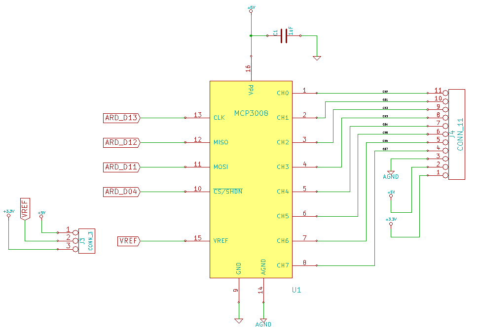
Schematic
Education Shield – MCP3800 ADC Subsystem
Setup
For this module, you’ll need the following equipment:
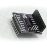
- I2C and SPI Education Shield or the MCP3008 Breakout Board
- Arduino UNO R3
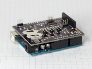
1. Mate the Education Shield with your Arduino UNO R3. If you’re using the MCP3008 Breakout Board, connect 5V to 5V, 3V3 to 3.3V, GND to GND, AGND to GND, CS to Digital4, MOSI to Digital11, MISO to Digital12, and CLK to Digital13. That’s a lot of pins!
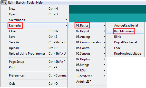
2. Connect your Arduino to your USB cable, and use the Arduino IDE to upload the “Bare Minimum” sketch from the Basics section of the Examples.
Preparing a Voltage Signal for the MCP3008 and your Arduino
We’re going to start off making single ended channel readings with the MCP3008. That means we should expect to get back some value that represents a voltage with 0 = Ground and 1023 = VREF. This also means that we’ll need something to measure.
The easiest thing to do is create a voltage divider, and the I2C and SPI Education Shield ADC header has 3V3, 5V and AGND all right next to each other, for you to use. You can use any combination of resistors to make a static voltage divider, but a potentiometer will allow us to make changes to the voltage and see them in real time.
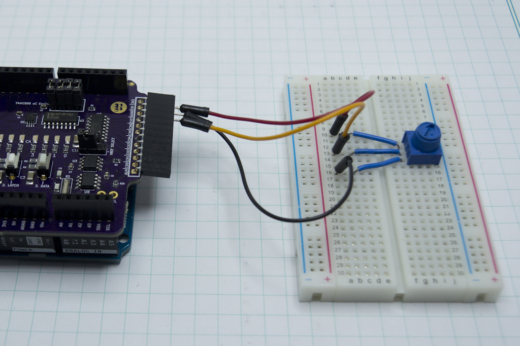
The connection then for the potentiometer to the ADC header is very simple. We’ll start with 5V, so run a jumper wire from 5V to one side of the pot, run a jumper wire from AGND to the other side of the pot, and then a final jumper wire from the middle pin to one of the input channels on the ADC header. I will be using CH7 in the code below, but there’s no difference other than the channel code we’ll send to the MCP3008, so feel free to change that.
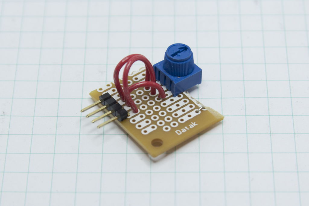
Because I changed out the connection to the ADC between different devices so many times while prototyping, testing and writing these education modules, I also soldered up a pot to a piece of perfboard so I can just whack it in there and test new code by reading CH7 and twiddling the pot knob.
This will give us a varying voltage to sample. It won’t be a particularly interesting voltage change, but it will change.
Sampling Voltage with the MCP3008 and your Arduino
With the potentiometer in place, it’s time to write our code. Let’s review quickly what we’ll need to do in the code to make sure it samples smoothly.
- Include the SPI.h library
- Specify our SPI configuration: speed, bit order and data mode
- Define the ADC CS pin and ADC related register addresses
- Send the start bit, SGL/DIFF bit, and CH Select bit in that order
- Wait for the sample to occur
- Capture the resulting values and display them
With that in place, we should be able to upload the code to the Arduino, twist the knob and see the values stream through the serial monitor telling us what voltage we’re getting.
Code Declarations
First and foremost, we have to include the SPI library, or none of this is going to work. This is such a common mistake for me to make, I wanted to call it out specifically. You can write out all your pseudo test code, refine, refine, refine, and then go to compile and generate a bajillion errors because you forgot to #include <SPI.h>.
|
1 2 3 4 5 6 7 8 9 10 11 12 13 |
#include <SPI.h> // Include the SPI library SPISettings MCP3008(2000000, MSBFIRST, SPI_MODE0); const int CS_MCP3008 = 4; // ADC Chip Select const byte adc_single_ch0 = (0x08); // ADC Single Channel 0 const byte adc_single_ch1 = (0x09); // ADC Single Channel 1 const byte adc_single_ch2 = (0x0A); // ADC Single Channel 2 const byte adc_single_ch3 = (0x0B); // ADC Single Channel 3 const byte adc_single_ch4 = (0x0C); // ADC Single Channel 4 const byte adc_single_ch5 = (0x0D); // ADC Single Channel 5 const byte adc_single_ch6 = (0x0E); // ADC Single Channel 6 const byte adc_single_ch7 = (0x0F); // ADC Single Channel 7 |
After our library include statement, we define the SPISettings, with 2Mhz (don’t know about you, but those zeros make it hard for me to read the value) clock frequency, most significant bit first bit order and a SPI mode of 0: CPOL0 / CPHA 0. We’ll use those with our SPI transaction statements in the body of the sketch.
The definitions are pretty simple. Chip Select is defined for the pin as digital 4, and then all the single ended channels are listed. The channel definitions already include the Single/Differential bit value, so we don’t need to worry about that later.
Now lets get setup rolling.
Setup
To no ones surprise, we’ll need to make sure the Serial communication is established, and run SPI.Begin() to dedicate the SPI pins to their activity. Forgetting to run SPI.Begin() is as common a mistake as forgetting to include the library in the first place. I’ve done it before… I’ll do it again. There isn’t much in the way of configuration for this chip, so rather than define a chip initialization function, as we’ve done so often in the past, we’ll just do the mechanical work of setting the CS pin mode and pin state so that it’s ready to go.
|
1 2 3 4 5 6 7 8 9 10 |
void setup() { SPI.begin (); Serial.begin (9600); pinMode (CS_MCP3008, OUTPUT); digitalWrite (CS_MCP3008, LOW); // Cycle the ADC CS pin as per datasheet digitalWrite (CS_MCP3008, HIGH); } |
We intentionally drive the CS pin low then immediately high just in case the chip powered up with the chip select floating somewhere in between. This forces a clean entry into the MCP3008 standby mode. Every chip is different, and reading the datasheet will tell you if you shouldn’t do this, but I find it a common practice to perform that ensures everything is ready to go.
Performing a Voltage Reading
To keep things clean, we’ll write a function that accepts the channel we want to sample as a byte parameter called readAddress, and returns the 10 bits of ADC data in the form of an integer. We’ll call the function “adc_single_channel_read”.
Since we’re going to use all 10 bits of returned data, you’ll recall we’ll need a sum total of 17 clock cycles to achieve that, and it all has to happen with the correct sequence. Let’s go step by step…
Voltage Reading Step 1: we need some place to put our returned data, and we commonly put those sorts of variables at the top of the function. We’re getting one and a quarter bytes of data back, so we’ll need one byte to hold the returned least significant byte and one byte to hold the most significant byte. In fact, those are good names for them: dataMSB and dataLSB. One last thing I want to define is our junk byte. Remember we have to send data even if all we want to is to receive data, and I’ll create a byte variable called “JUNK” with a value of 0x00 just so it’s plainly obvious what’s going on.
|
1 2 3 |
byte dataMSB = 0; byte dataLSB = 0; byte JUNK = 0x00; |
Voltage Reading Step 2: we have to prepare the SPI bus for our interaction. Now, since we’re only dealing with one chip, and we’re not planning on using the SPI bus for any activity other than SPI, we don’t necessarily need to do this here, but to make it clear what’s happening, we’ll be as verbose with our code as possible, even though it may be at the expense of performance.
|
1 |
SPI.beginTransaction (MCP3008); |
The command is referencing the MCP3008 SPISettings object we instantiated in the declarations section.
Voltage Reading Step 3: drive the CS pin low to tell the MCP3008 to get ready for business time.
|
1 |
digitalWrite (CS_MCP3008, LOW); |
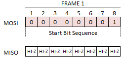
Voltage Reading Step 4: the chip is ready so the time has come to do some SPI transactions. There are a number of ways of doing this, but I’m going to sequence everything so that the last bit of valid data is located in the last bit of data transmitted. That means we have to shove everything over to the right by 7 clock cycles. We could do this by sending out the start bit right away, but then we have a bunch of trailing zeros that have to be dealt with. Not impossible at all, but I think this makes for greater clarity. So how do we “shove everything over by seven clock cycles”? By ensuring our start bit is the last bit transmitted in the first frame. That means sending out the value B00000001, hex value 0x01. That makes the first frame of SPI interaction look like this (Hi-Z means the pin is in a high impedance state — it’s as though it doesn’t exist on the PCB).
|
1 |
SPI.transfer (0x01); |
The chip now needs to receive the Single/Differential bit and Channel selection bits, which we already combined in the declarations section, and will be passing to the function as the value “readAddress”. Remember though that the transmission is sent MSB first, and we defined the channels as their discrete bit value. So for Channel 7, the value is B0001111, hex value 0x0F. If we just sent that, we’d start off with a bunch of zeros, so we’ll need to shift the address over by four places. It’s sort of user’s preference as to whether you want to define the channel with four bits in the MSB or LSB position, but with our sequence the bits in question need to be at the start of the frame, not the end. It’s not quite as simple as just sending that value either. SPI is bidirectional, and the MISO line is going to start chirping as soon as the sample wait time is completed. This is what we would expect to have happen…
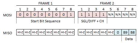
In 8 bits we’re sending data out on MOSI and receiving data in on MISO. That means we have to put the value we send out inside the SPI.transfer() function, and capture the return. But, but, but… the returned value could contain some funky data in the most significant five bits when MISO is in a Hi-Z state, so we need to mask all of that off. We only want to keep the last two bits of that incoming value, so we’ll AND it with B00000011, hex value 0x03. Since the data being sent is coming out of the chip Most Significant Bit first, we’ll put this into our dataMSB variable. Lotta stuff going on in one command.
|
1 |
dataMSB = SPI.transfer(readAddress << 4) & 0x03; |
Now we need to grab the remaining eight bits of data. This is a little easier, than the last command. We don’t care about the data we’re sending, so we’ll just send junk data, and the data we’re receiving is entirely valid, so we don’t have to mask any of it off.
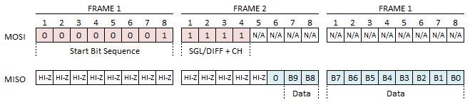
This is the least significant eight bits of data, so we’ll put it into the dataLSB variable.
|
1 |
dataLSB = SPI.transfer(JUNK); |
Voltage Reading Step 5: All our SPI stuff is done, so put the chip back into standby and open up the SPI bus to interact with other chips by bringing the ADC chip select pin back high.
|
1 |
digitalWrite (CS_MCP3008, HIGH); |
Voltage Reading Step 6: For the sake of completeness, we’ll go ahead and end the SPI transaction, which allows the SPI bus to be configured in some other fashion now. We don’t have to do this because, again, we’re only interacting with a single chip, but it’s good to get into the habit.
|
1 |
SPI.endTransaction (); |
Voltage Reading Step 7: We’ve retrieved our data from the MCP3008 and have it stored in two different byte variables. Now we need to mash the two together so that the MSB data goes to the left and the LSB data goes to the right — 10 bits of data in total, so we can’t store it all in a single byte, that’s why the returned value is an integer. With a little bit shifting and bit masking, we can accomplish the goal.
First take the dataMSB variable and move it 8 places to the left…
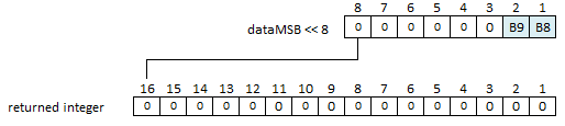
…then OR the resulting value with the dataLSB variable, which will drop that data into right most 8 bits…
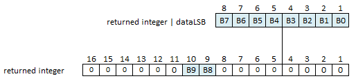
…and throw all of that back as the returned value…

|
1 |
return dataMSB << 8 | dataLSB; |
Take all seven of those steps and put them together to get the following complete function…
|
1 2 3 4 5 6 7 8 9 10 11 12 13 14 15 16 17 18 |
int adc_single_channel_read(byte readAddress) { byte dataMSB = 0; byte dataLSB = 0; byte JUNK = 0x00; SPI.beginTransaction (MCP3008); digitalWrite (CS_MCP3008, LOW); SPI.transfer (0x01); // Start Bit dataMSB = SPI.transfer(readAddress << 4) & 0x03; // Send readAddress and receive MSB data, masked to two bits dataLSB = SPI.transfer(JUNK); // Push junk data and get LSB byte return digitalWrite (CS_MCP3008, HIGH); SPI.endTransaction (); return dataMSB << 8 | dataLSB; } |
Calling our Single Channel Read and Showing Value with Voltage
The value has been received now and it’s up to us to decide what to do with it. For this first sketch, all we’ll do is spit it out to the serial monitor. However, we may as well add a little formula that will translate the 10 bit value we’re receiving back into a comprehensible voltage.
The first thing we need is a true value for our VREF. Now this is dependent on how you’re powering your Arduino, unfortunately. I didn’t place a discrete voltage reference component on the board; VREF is just pulling 5V (or 3V3) from the main power rails of the Arduino. If you’re powering the UNO from the USB connection on your computer, you won’t see true 5V, because the USB power is 5V, and it’s passing through a voltage regulator, so you end up with something less than that. If you power it off the 9V battery jack, then you get a solid 5V. It’s worth grabbing your multimeter to confirm the value. Powered off the USB jack of my PC, my 5V rail measures closer to 4.91V, so that’s the value I’ll use for my VREF calculation. It’s very easy to measure the rails, using the test points right by the battery holder.
We’ll need an integer to store our returned value from adc_single_channel_read, and after that, we issue the command and do some serial printing and math and we’re done.
|
1 2 3 4 5 6 7 8 9 10 11 12 13 14 15 16 |
void loop() { double vRef = 4.91; int adc_reading = 0; adc_reading = adc_single_channel_read (adc_single_ch7); Serial.print ("ADC Ch "); Serial.print (adc_single_ch7 & 0x07); Serial.print (" Voltage: "); Serial.println ((adc_reading * vRef) / 1024, 4); delay(50); } |
The only trickery in there is taking the measured channel and “&” it 0x07. That eliminates the SGL/DIFF bit from the front of the channel selection bits, and it turns out the remaining bits are the hex value of their regular ol’ decimal name. Then in the last serial print command, we’re taking the adc_reading multiplying it by the value we determined for vRef and dividing it all by 1024, which happens to be the formula printed in the datasheet. The “,4” part at the end, specifies how many decimal places we want to show. Since each step is 0.0048V, I figure it’s worth it to out that far. Tighten up as you see fit. (Honestly, I’m a little surprised this code doesn’t throw a variable type mismatch error, trying to multiply an integer with a double. I’m also a little surprised that the resulting output is of type double and not type integer, but not surprised enough to really care at this point.)
The delay(50) at the end is just to make it easier for me to make screen captures of the serial monitor window. You don’t have to include it.
The whole kit and caboodle put together comes out to this…
|
1 2 3 4 5 6 7 8 9 10 11 12 13 14 15 16 17 18 19 20 21 22 23 24 25 26 27 28 29 30 31 32 33 34 35 36 37 38 39 40 41 42 43 44 45 46 47 48 49 50 51 52 53 54 55 56 57 58 59 60 61 62 63 64 65 66 67 68 69 70 71 72 73 74 75 76 77 |
/* A sketch to control the 10-Bit, 8-channel ADC MCP3008 on the Rheingold Heavy I2C and SPI Education Shield. The code supposes the use of the Education Shield, but if you're using a breakout board, connect the CS pin to Digital 4, and the SPI pins in their usual locations. Website: https://rheingoldheavy.com/mcp3008-tutorial-02-sampling-dc-voltage/ Datasheet: http://ww1.microchip.com/downloads/en/DeviceDoc/21295d.pdf */ #include <SPI.h> // Include the SPI library SPISettings MCP3008(2000000, MSBFIRST, SPI_MODE0); const int CS_MCP3008 = 4; // ADC Chip Select const byte adc_single_ch0 = (0x08); // ADC Channel 0 const byte adc_single_ch1 = (0x09); // ADC Channel 1 const byte adc_single_ch2 = (0x0A); // ADC Channel 2 const byte adc_single_ch3 = (0x0B); // ADC Channel 3 const byte adc_single_ch4 = (0x0C); // ADC Channel 4 const byte adc_single_ch5 = (0x0D); // ADC Channel 5 const byte adc_single_ch6 = (0x0E); // ADC Channel 6 const byte adc_single_ch7 = (0x0F); // ADC Channel 7 void setup() { SPI.begin (); Serial.begin (9600); pinMode (CS_MCP3008, OUTPUT); digitalWrite (CS_MCP3008, LOW); // Cycle the ADC CS pin as per datasheet digitalWrite (CS_MCP3008, HIGH); } void loop() { double vRef = 4.91; int adc_reading = 0; adc_reading = adc_single_channel_read (adc_single_ch7); Serial.print ("ADC Ch "); Serial.print (adc_single_ch7 & 0x07); Serial.print (" Voltage: "); Serial.println ((adc_reading * vRef) / 1024, 2); delay(50); } int adc_single_channel_read(byte readAddress) { byte dataMSB = 0; byte dataLSB = 0; byte JUNK = 0x00; SPI.beginTransaction (MCP3008); digitalWrite (CS_MCP3008, LOW); SPI.transfer (0x01); // Start Bit dataMSB = SPI.transfer(readAddress << 4) & 0x03; // Send readAddress and receive MSB data, masked to two bits dataLSB = SPI.transfer(JUNK); // Push junk data and get LSB byte return digitalWrite (CS_MCP3008, HIGH); SPI.endTransaction (); return dataMSB << 8 | dataLSB; } |
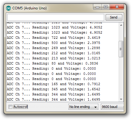
Upload that code and then open your serial monitor. As you see twist the dial on your potentiometer, you’ll see the voltage increasing and decreasing.
Predict and Experiment
Without modifying your code or the wiring, what do you think will happen if you change to the 3V3 VREF from the 5V and run your code again?
Hover to read answer
Without modifying your code, what do you think will happen if you change to the 3V3 VREF from the 5V, and connect your potentiometer to 3V3 on the ADC header then run your code again?
Hover to read answer
Without modifying your code, what do you think will happen if you select 5V VREF, and connect your potentiometer to 3V3 on the ADC header then run your code again?
Hover to read answer
What part of your code will need to change whenever you select a new value for the voltage reference?