Welcome to the MCP7940 Real-Time Clock/Calendar from Microchip. This module will cover the functionality of the chip based on the datasheet.
Objectives
- Understand the various operating characteristics of the MCP7940.
- Understand the features of the Multi-Function Pin.
- Understand how the battery backup works.
- Understand how the time is calibrated.
- Understand how the alarms work.
- Understand how to access the 64bytes of SRAM.
Background
I2C Signaling
How To Read A Datasheet
Microchip MCP7940 Datasheet
Schematic
Education Shield – MCP7940 RTCC Subsystem
Setup
There is no setup required for this module.
MCP7940 Functionality Overview
The MCP794N is a Real Time Clock/Calendar, RTC, device. It takes the regular pulses from the connected 32.768kHz crystal and a start time and date specified by you, and starts tracking the time and date just like a regular watch. In addition to the basic time and date keeping features of the MCP7940, it also has a pair of alarms that can trigger interrupts, a battery backup subsystem to maintain the clock and date values if power is lost, a pin that can output the alarm interrupts, a variety of specific PWM signals or even just work as a general output pin, and 64bytes of SRAM available for R/W duties.
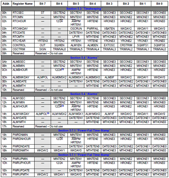
Looking at the register map for the RTC, you can immediately tell that it’s a bit more complicated to work with than the temperature sensor we’ve been dealing with so far.
Time and Date
Time and date are maintained in a series of R/W capable registers with one register used for each property of a time stamp: second = 0x00, minute = 0x01, hour = = 0x02, etc. There are configuration bits sprinkled throughout the time/date registers, so you have to be very, very careful when both reading and writing from the registers.
The individual time and date values are what you would expect them to be, with the only funky one being the “WEEK DAY” value. It’s simply a number from 1 to 7 that increments every 24 hours and rolls over from 7 to 1. It’s up to you to assign some meaningful value to that in code such as “MONDAY, TUESDAY” etc. Personally, I think you should name the days of the week, “RHEINGOLD”, “HEAVY”, “IS”, “AWESOME”, “SO”, “AM”, “I”, and we can all look forward to three day weekends when we try to sneak out of work early on AM and can take HEAVY off to barbecue.
The timestamp values are stored in a method called “Binary Coded Decimal”, which for the purposes of the MCP7940 means that the one’s place of the particular value is represented by the least significant four bits of the register, and the tens place is located in the most significant four bits of the register. Since none of the time values will exceed the value of 6, B0110, that leaves a lot of extra room in the MSB positions, which is why configuration bits seem to be randomly spread throughout… that’s Microchip making the most of the space at hand.
Because there can be small variations between different crystal oscillators, and in the environments that the chip might be used in (temperature causing significant variations in oscillator output), the MCP7940 provides a way to trim the speed at which the clock runs using the OSCTRIM register, by adding or subtracting clock cycles from the regular quantity that comprise a single second. By comparing how long it takes for the clock to run against a standardized time source, you can calibrate the clock to be accurate over the long term.
Multi-Function Pin
The Multi-Function pin is tied to Digital3 of your Arduino through the Education Shield. Digital3 is also usable as Interrupt1 (the alarm pin of the AT30TS750A is tied to Interrupt0). The MFP has three modes it can be used in:
- Alarm Interrupt: When one of your configured alarms is reached, the chip will change the polarity of the MFP, based on the configuration of the ALMPOL bit in the ALM0WKDAY register. In this way, it is easy to immediately execute some code based on a human recognizable time and date.
- Square Wave Output: The pin is able to function as a PWM generator, pulsing at 1Hz, 4.096kHz, 8.192kHz and 32.768kHz. These can be used to do things like blink an LED once a second, or generate a variety of alarm tones if desired.
- General Output: The MFP is an Open Drain pin, so it resides at 5V by default. It can be driven to GND if desired by setting the OUT bit in the CONTROL register.
Battery Backup
A CR2032 LiON battery can be used to act as a backup power supply which will maintain the time and date values with the power disconnected for limited lengths of time. When operating off of backup power, several features are disabled to reduce the current draw and preserve battery capacity. According to the datasheet, the following are maintained when running off of battery power…
- Timekeeping
- Alarm Values
- Alarm Output
- Oscillator Trimming
- RTCC Register and Contents of the SRAM
The following features are disabled when running off of battery power…
- I2C Functionality
- Square Wave MFP Output
- General Purpose MFP Output
If the VBATEN bit is set in the RTCWKDAY register, then a timestamp is logged on both power failure and power restoration in the PWRDNXX and PWRUPXX registers respectively. When the PWRUPXX registers are written to, the PWRFAIL bit is set by the chip to 1 and must be cleared in order to reset the PWRDNXX and PWRUPXX registers to 00:00:00 00/00/0000.
Alarms
The MCP7940 has two alarms, ALM0 and ALM1. When the comparator detects a match between the alarm and the current time, it will set the ALMxIF bit and, provided the MFP is not tasked with square wave output, it will assert the pin to the polarity state specified in ALMPOL.
The comparator will set an alarm based on a recurring second, minute, hour, day of week, date or full time stamp, based on the selected alarm mask specified in the ALMxMSK bits in each ALMX register. Using code, you can easily implement an alarm clock, snooze features, etc. that will trigger code to execute through the interrupt sequence. Pretty cool, actually 🙂
64bytes SRAM
The additional SRAM located inside the RTC device is accessible as a separate block of registers, 0x20 – 0x5F, but is called using the same I2C address. Each register is 8-bits wide and there are 64 of those registers = 64 bytes. The registers can be R/W accessed either randomly or sequentially:
- Random Access: random access means that you would specify the register address you want to read or write from anywhere within the memory space allocated to the SRAM, then write the data. This is similar to the sequences we’ve dealt with so far, where you send the I2C address, send a register address, read or write the data you want, then issue a Stop Condition.
- Sequential Access: with sequential access, you only have to specify a register address the first time, and then you keep pinging the RAM with read requests, never having to issue a stop command until you’re done. The internal pointer on the RTC module just advanced one byte each time it finishes accessing a byte of memory. You have to be careful though, because if you get to 0x5F and try to write another byte of data, you’ll roll over to the beginning of the SRAM block, 0x20 and start to overwrite anything in there.
