This module provides detail on the I2C signals, the conditions established at each step in the signaling process, and detailed timing for each.
Objectives
- List the different steps of an I2C transaction
- Understand the timing requirements of each step
- List the reasons why a NACK might be transmitted
- Determine if I2C is an MSB or LSB first technology
- Describe the difference between a stop condition and a repeated start
- Understand what is meant by clock stretching
Background
I2C Basics
Reading through the previous sections will be helpful for the less experienced, but are not necessarily essential.
Schematic
No schematic is associated with this module.
Setup
This module is dedicated to I2C theory, so no hardware is necessary at this point.
I2C Signals
There are two signals that govern all I2C communication: the serial clock signal SCL and the serial data signal SDA. While either the master or slave components are able to manipulate the state of the SDA bus at the appropriate time, the SCL signal is always generated by the master.
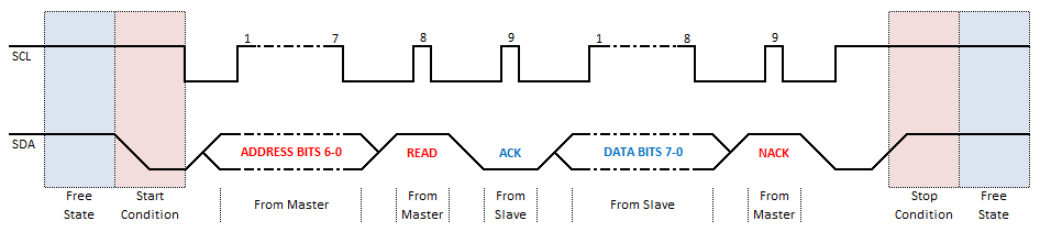
In a basic one byte transmission of data over I2C to the master component, a very specific sequence of steps needs to occur.
- First the bus must be in a free state
- A start condition is established by the I2C master
- An address is transmitted by the I2C master
- A R/W flag is transmitted by the I2C master
- An ACK/NACK (hopefully an ACK) is transmitted by the I2C slave
- 8 bits of data are transmitted
- An ACK/NACK (hopefully a NACK) is transmitted by the I2C master
- A stop condition is established by the I2C master
- The bus returns to the free state
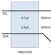
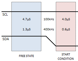
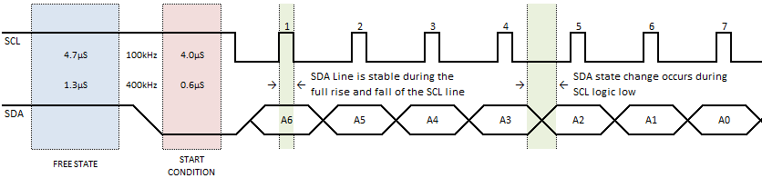
Free State
The I2C Free State is established when both the SCL and SDA lines are held at the logic high state. In the case of the Arduino, that would mean 5V. The length of time the bus must be held in the free state is designated tBUF and is 4.7µS at 100kHz and 1.3µS at 400kHz.
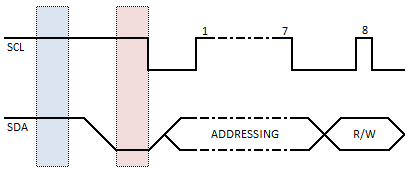
Start Condition
When the master is ready to initiate communication on the I2C bus, it creates a start condition, by transitioning the SDA line low while holding the SCL line high. The length of time the bus must be held in the start condition is designated tHD;STA and is a minimum 4.0 uS at a 100kHz bus speed and 0.6uS at 400kHz.
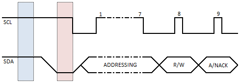
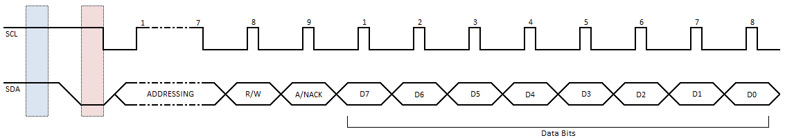
Address Transmission
Once the start condition has been established by the master, which tells the slaves to start listening, the master begins transmitting the 7-bit address on the SDA line, one bit per clock cycle. The SDA line must remain in its state during the full clock cycle in order for the data to be considered valid. During data transmission (meaning that establishing the start and stop conditions don’t count), the SDA line may only change state when SCL is at a logic low state. The address is always sent MSB first.
READ/WRITE Flag
Immediately after the 7-bit address has been sent, a Read / Write flag is sent, which specifies which direction data will be flowing. R is active high, so 1 in the R/W flag indicates that the master is requesting data from the address. W is active low, so 0 in the R/W flag indicates that the master is sending data to the address.
ACK/NACK Flag
After the address and R/W flag are sent, the master releases control of the SDA line and pulses the SCL bus to signal the slave component corresponding with the address to respond with an acknowledgement “ACK” or a non-acknowledgement “NACK”. When the master receives the ACK, it prepares to send or receive data based on the previously sent R/W flag. This is the ninth bit in every I2C transmission and it can seem odd if you’re not prepared to see it, since it’s easy to become accustomed to seeing 8 clock pulses. With I2C, the ninth clock is always the ACK/NACK.
The I2C Manual establishes five conditions in which a component may respond with a NACK…
- There isn’t anything on the I2C bus that corresponds to the address that was sent. Since no one’s home, there’s nothing to pull the SDA line low, so a NACK is registered.
- The device that is responsible for issuing the ACK is busy doing something else and can’t respond. For example, an ADC may need time to generate it’s voltage measurement before it can acknowledge that it’s ready to transmit a value, in that case it would leave the SDA line high to indicate NACK.
- During transmission, if the device receiving the data doesn’t know what to do with what it’s receiving, it will respond with a NACK at the end of that byte of data.
- During transmission, if the device receiving the data can’t accept any further data, it will send a NACK and tell the transmitter to shut up.
- The master, when having data sent to it, needs to signal the end of the communication with the slave transmitter. It does this by issuing a NACK at the end of the last byte.
The ACK/NACK after the address is transmitted is always sent by the slave. The ACK/NACK during data transmission is set by which ever device is receiving the data. If the slave is receiving the data, you should expect to see ACKs up to the very last bit is sent. If the Master is receiving the data, it will set a NACK after it has received all the data it wants, telling the slave to stop transmitting.
Remember, ACK is sent by pulling SDA low… because of the open drain configuration of the I2C bus, you have to be an active participant to create a logic low state.
Data Transmission
Provided the ACK was sent after the address and R/W bits, data will now start flowing dependent on the direction specified by the R/W flag. Data on the I2C bus is always sent in bytes comprised of 8-bits. If you’re dealing with a component that needs to send more or less than that, a 10-bit ADC for example, the datasheet will inform you that the 8-bit frame containing the extra data will be padded either with something else, like config information, or junk data that is ignored, and it’s up to you to reassemble the data appropriately in software. Data is always sent MSB first.
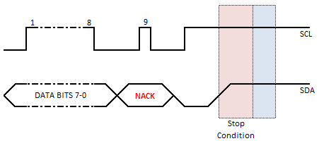
Ending Transmission – Stop Condition
At the end of each byte of data, the receiver is responsible for issuing an ACK/NACK byte in the ninth clock cycle, to indicate that it’s either ready to receive another byte of data, or it is done communicating. If the ACK is sent, another byte of data is sent and it continues in this fashion, ACK + 8bits + ACK + 8bits until either the master is finished transmitting or the master sets a NACK if it is receiving.
When the transmission is finally issued, several things can happen. Firstly, the master can establish a stop condition, indicating that the I2C bus is transitioning from the busy state back to the free state. The setup and hold times for the stop condition are identical to those specified for the start condition, with the exception being that the SDA line is transitioning from logic low to logic high as the SCL bus is held high.
All assembled, a full request and transmission of a single byte of data from the slave to the master looks like this…
Continuing Transmission – Repeated Start
After a full byte of data has been sent and the receiving device sends the NACK to indicate completion, the master can choose to repeat the start condition rather than enter the stop condition and enter the free state. This allows the master to maintain control of the bus and go straight back to selecting a device to communicate with instead of possibly having to wait for another master to release control of the bus. Repeated Start conditions are typically only necessary in multi-master architectures.
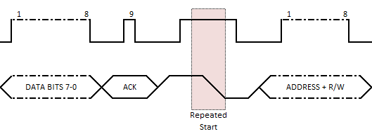
The way to differentiate between the stop condition and the repeated start condition, is that in the stop condition, the data signal goes high AFTER the clock does. In the repeated start condition, the data signal goes high BEFORE the clock does, then drops under a high clock to initiate the repeated start.
Clock Stretching
If during the course of a data transmission, a transmitting device needs more time before the next bit needs to be sent or received, it can perform a technique called “clock stretching”. This is the only instance in which a slave device can grasp control of the clock signal.
Essentially, the device that needs the extra time holds the clock line low, preventing any further transmissions on the I2C bus, until the device is ready, releasing the line to go high and allowing communication to continue.
This is useful if you’re receiving data at a high rate on your I2C bus, but need to press the pause button on the incoming data to write your buffered data to more permanent but slower storage. As soon as your buffer is emptied, you let the clock line go high and start reading again.
Multi-Master Configuration
There may be instances where it is necessary to have multiple master devices communicating on the same I2C bus. The specification allows for this through the use of clock synchronization and an arbitration scheme.
Before arbitration can begin, the bus must be in the free state. Then, if both masters successfully establish a start condition simultaneously, they will continue on with their communications scheme: addressing, R/W, ACK/NACK, etc. However, the first time that a master attempts to let the SDA line go to logic high but detects that it remained in a logic low state, it will realize in it’s silicon bones that it has lost the arbitration and it disables itself until a free state is established on the bus again.
For the clocks to synchronize, a low state is generated by one of the masters on the bus. At this point, both masters begin counting the length of time designed into their logic for a valid low state. The first master to reach the end of the count attempts to raise the line high, but can’t and enters a wait state while the additional master keeps the line low. Eventually that second master reaches it’s count and lets the line go high and both masters begin their high count simultaneously. When the master with the shortest high count is ready, it brings the line low again and the cycle repeats. The clock signal period is thus dictated by the master with the longest low period and the master with the shortest high period.
Greater detail on the design and implementation of a multi-master I2C design is beyond the scope of this course, but can be researched easily. I recommend reading the surprisingly user friendly I2C-bus Specification and User Manual from NXP as a good starting point.