Our inputs are going to be just like they’ve been so far, a pair of mechanical switches connected to SET and RESET. We are going to determine when we’re going to take a sample of our inputs using something called a “clock signal”, that’s our heartbeat. Ideally, it would be a regular HIGH/LOW square wave, ticking away at a regular basis like a clock, but to start with, we’re just going to use another switch so we can keep things slow enough to comprehend.
Basic Clocked SR Flip Flop
Bare with me just a bit because this first example is pretty damn impractical. Essentially, what we’re going to do is inject our clock signal into the system, but still have the SET and RESET inputs to manage, and an indeterminate state to avoid. This will get better but this is the necessary first step towards that.
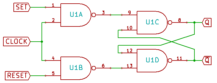
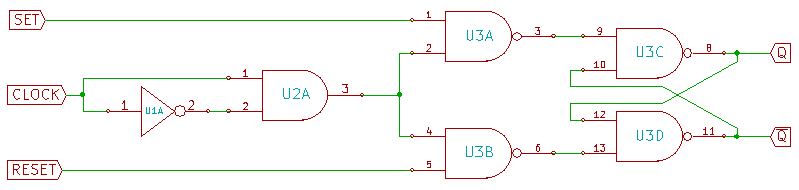
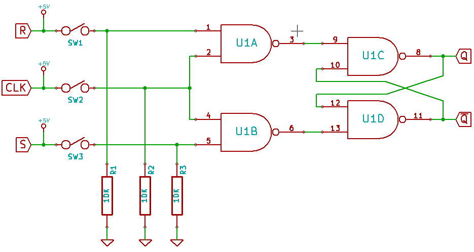
What we have on the right, is the basic NAND based SR Flip Flop from before, but we’re adding a pair of NAND gates on the inputs and tying one input from each together. That unified input becomes our CLOCK, while maintaining separate SET and RESET inputs. Because our signals are passing through those two NAND gates before we get to our flip flop, they are essentially being inverted, so unlike our basic NAND gate flip flop where the inputs were active low, they are now active high. We’ll refer to them again as SET and RESET.
This is best illustrated by using a truth table and some more of my certified amazing schematic slideshows.
| SET | RESET | CLOCK | Q | NOT-Q | STATE |
|---|---|---|---|---|---|
| LOW | LOW | LOW | Q | NOT-Q | HOLD |
| LOW | HIGH | LOW | Q | NOT-Q | HOLD |
| HIGH | LOW | LOW | Q | NOT-Q | HOLD |
| HIGH | HIGH | LOW | Q | NOT-Q | HOLD |
| LOW | LOW | HIGH | Q | NOT-Q | HOLD |
| LOW | HIGH | HIGH | LOW | HIGH | RESET |
| HIGH | LOW | HIGH | HIGH | LOW | SET |
| HIGH | HIGH | HIGH | HIGH | HIGH | INDETERMINATE |
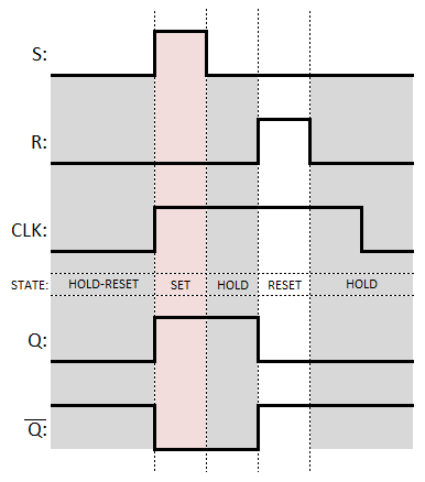
That’s a lot of hold states! Essentially, while the CLOCK signal is low, you’re not going to change the output at all, that means that you will only set the state of the outputs when CLOCK is high, which makes sense. Once CLOCK is high, then the SET and RESET states are exactly as we would expect for non-inverted inputs.
In this slide show, we start with the flip flop in the RESET state (remember, to avoid an indeterminate state, we have to establish a valid state to start with). First the inputs pulse with CLOCK held low, resulting in HOLD-RESET. Then the CLOCK pulses with the inputs low, HOLD-RESET maintaining. Finally the process flows through from RESET to SET (trying to present each state made this ungainly to watch so I’ve limited it to just demonstrating the one state change.)
[masterslider id=36]Building a Clocked SR Flip Flop
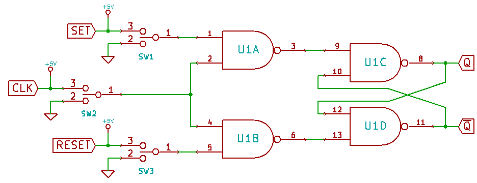
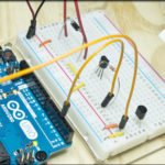
This is about the last of the circuits that you can build with tactile buttons, so if you want to do so, use a modified schematic as we’ve done in the past, remembering to provide pull down resistors on all three inputs.
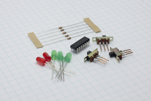
After putting it together with a couple of extra jumper wires than we’ve needed to this point, here it is in action.
[masterslider id=37]
Edge Triggering
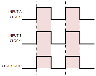
There is a drawback to the above design in that the clock is “level triggered”: when the clock is at the high level, SET and RESET can bounce all they want and the outputs will swap accordingly and instantly. That results in a timing diagram that looks like this…
When CLOCK is high, you see SET and RESET toggle, putting you back into a RESET condition because those inputs are valid for the entire time the CLOCK is held at that level. What we need to do is sample the inputs only at the exact moment when the clock is transitioning from low to high (or from high to low). This is called “edge triggering” because you are triggering the flip flop only at the edge of the clock signal.
We accomplish this by introducing a microscopic delay, on the order of nano-seconds, in the transition of the clock signal during which we care what the state of the inputs is. This starts to require a large number of logic gates to build the individual flip flops, so I’ll just concentrate on how we modify the clock signal, because the rest of it is essentially the same.
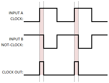
There are many different ways of edge triggering, but I think this is the simplest way of communicating the concept. In the above circuit, the clock inputs on the NAND gates are instantaneous, so when the clock goes high, it goes high in both places at the same time, and stays that way until you bring the clock low. In order to tighten that up, we create a delay by initially splitting the clock signal through an inverter first, then a subsequent AND gate, before it goes into our flip flop.
While our CLOCK signal is low, everything is in a steady state: the input to the top of the AND gate is low and the input to the bottom is inverted, so the output is high. Now, we bring the CLOCK signal high. This is immediately reflected at the top input of the AND gate, and for a split second, tens of nanoseconds, you get a high on both inputs of the AND gate generating a high output. You exploit the fact that it takes time, miniscule to be sure but time nonetheless, for the NOT gate to flip that bottom signal low. This is called propagation delay. In that barest hint of a moment before the NOT gate turns the AND gate off again, you successfully trigger the flip flop off to sample the inputs.
It may require several inverters in order to establish the sufficient delay required for all the signals to actually settle at their high values for the required delay, I only used one in the schematic as an example.
What we’ve created is a “positive edge triggered” flip flop or “leading edge”, because you are triggering the flip flop as the clock signal goes from low to high. A “negative edge triggered” or “trailing edge” flip flop can be created by replacing the AND gate with a NOR gate.
Here is a timing diagram for the AND gate without the inverter…
Now, after we put the delay in, this is what we are hoping to achieve…
In order to build the delayed clock signal, you just start daisy chaining the inverters together until you achieve the required length of high pulse specified by the datasheet.
Looking at the SN74HC08 datasheet, on page 3 it lists a “High-level input voltage” of 3.15V (the level you have to get for it to register as high), and a “Maximum Input transition rise or fall rate” of 500ns, that’s how long it could take for the gate to switch from one state to another — we know then, that we’ll need to be looking down at the nanosecond scale to ensure we’ve got a long enough pulse.
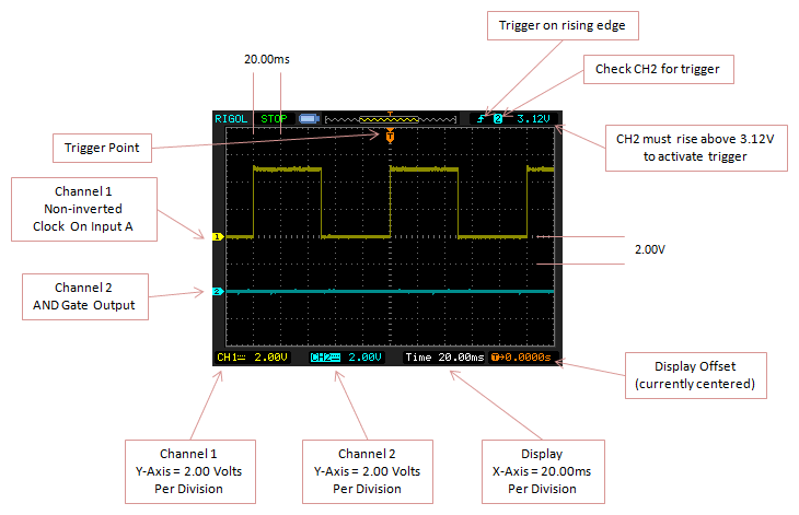
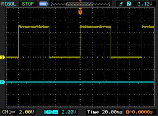
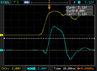
To examine this theory, I used my Arduino to generate a clock signal (covered below), of 50ms on / 50ms off, cycling back and forth. I’ve also hooked my oscilloscope up to look at what’s happening to the AND gate output versus the CLOCK signal coming from the Arduino. Oscilloscope Channel 1 is the CLOCK signal, sampled at Input A of the AND gate. Oscilloscope Channel 2 is the output of the AND gate. Input B of the AND gate is not shown on the scope, but is being directed through a a single NOT gate to create the propagation delay.
1. Overview
With a time division of 20ms, it appears that we have a nice square wave lasting 50ms high and then 50ms low. Channel 2 though, just looks flat at 0V (I moved it down the display from the center so that it could be compared to Channel 1 easily). Remember though, that the gates transition in nanoseconds, not milliseconds, so we need to tighten the time up a little bit.
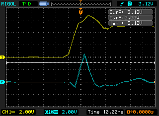
2. Zoomed in to 10 nanosecond scale
Now we see something happening. The time divisions are now 10 nanoseconds (each little dot is 2ns, each column is 10ns). The resolution of my scope isn’t all that tremendous down at this speed, but you can definitely see a spike occurring at the output of the AND gate (Channel 2). It’s only lasting around 2 nanoseconds though and I’m not confident that’s going to be long enough to get the gate to register a valid high state on input B. Let’s add another NOT gate.
3. Input With Two Inverters
CLOCK is now running through two NOT gates before it arrives at Input B of the AND gate. Unfortunately, since we’re inverting the signal, then inverting it again, we wind up mirroring the CLOCK entirely. You can’t generate an UP-DOWN pulse with even numbers of NOT gates, it must be an odd number. So let’s add another one.
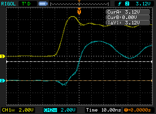
4. Input With Three Inverters
I’ve added a third inverter, and now that we have an odd amount, we can see that the signal goes low again. The good news is that the length of the pulse is much longer than it was with one NOT gate. The white line bisecting the hump like Roy Neary trying to build Devil’s Tower, is a guideline I’ve set for the minimum voltage necessary to register high, 3.15V. We’re staying above that line for around 14ns. I bet this is long enough, but let’s add one more inverter just to be sure.
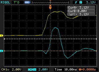
5. Input With Five Inverters
Five inverters strong now, and we’ve got a full 20ns pulse width created.
To verify, I set the scope to acquire 256 samples of the delay and average them out so I’d get a clearer picture of what we were getting over time. Sure enough, a full 20ns was spent at the AND gate output above the minimum required 3.15V high Level.
It should be noted that the delay generated by the NOT gates offsets the AND gate output from the actual clock signal by about 10ns in the final example. That length of time might appear tiny on human scale, and in many electronics applications it is, but if you start talking about trying to flip that flop on a gigahertz scale, it would become an issue. That said, if anyone is trying to create gigahertz scale registers using 15 year old 7400 series logic gates in DIP footprints jammed into a breadboard, I’d love to see it. I wouldn’t love to do it… but I’d love to see it.
Clock Signal Generators
Now that we’re starting to talk about edge triggering, the effects of “switch” or “button” bounce on our clock signal are going to become impossible to deal with. Let’s replace the clunky mechanical switch that we’ve been using to generate our clock with a nice clean electronically generated one.
We need to define some terms first…
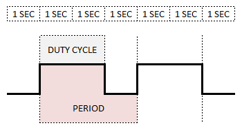
Period The period of a signal is the time required for the signal to complete a full ON/OFF cycle.
Duty Cycle The percentage of time during which that signal is in an active state. So looking at that diagram, the period is 3 seconds, and the duty cycle is 2 seconds.
Frequency this describes how many times something happens within a standardized one second’s length of time. It is also the inverse of the period, \(F = \frac{1}{P}\). Think of it this way, the period above shows that something is happening for three seconds length of time, which means that in the standard span of one second, only 33% of that something has had a chance to happen, meaning a frequency of .33Hz.
If it happens once in one second, we are going to call that “one hertz” or 1Hz. If it happens 1,000 times in one second, then it’s one kilohertz (1KHz), and so on.
I hope that makes sense, because it baffled the hell out of me for quite a while.
To put all of that into something practical, we are going to want to sample our input switch once per second, and store it’s state on the output until we sample again. The trigger to sample will be our clock signal. In order to let us perceive what’s going on, we want to make sure the frequency of our clock signal is nice and slow, at least 1Hz or slower with a 50% duty cycle (half a second on / half a second off).
First, here’s some code you can use to generate a simple, slow, clock from your Arduino…
|
1 2 3 4 5 6 7 8 9 10 11 12 13 14 15 16 17 18 19 20 21 22 23 24 25 26 |
/* Simple 1Hz Clock Signal Generator Adjust the delays in the main loop to increase or decrease the frequency of the signal. http://www.rheingoldheavy.com */ int clockPin = 2; // clock output on digital pin 2 void setup() { pinMode(clockPin, OUTPUT); // Sets the clock pin as an output } void loop() { digitalWrite (clockPin, HIGH); // take clock signal HIGH delay (500); // wait for half a second digitalWrite (clockPin, LOW); // take clock signal LOW delay (500); // wait for half a second } |
All we do is write Digital 2 high for half a second, then write it low for half a second… again and again and again and again.
Alternatively, you can use a 555IC to generate a simple clock signal as well, using the following schematic…
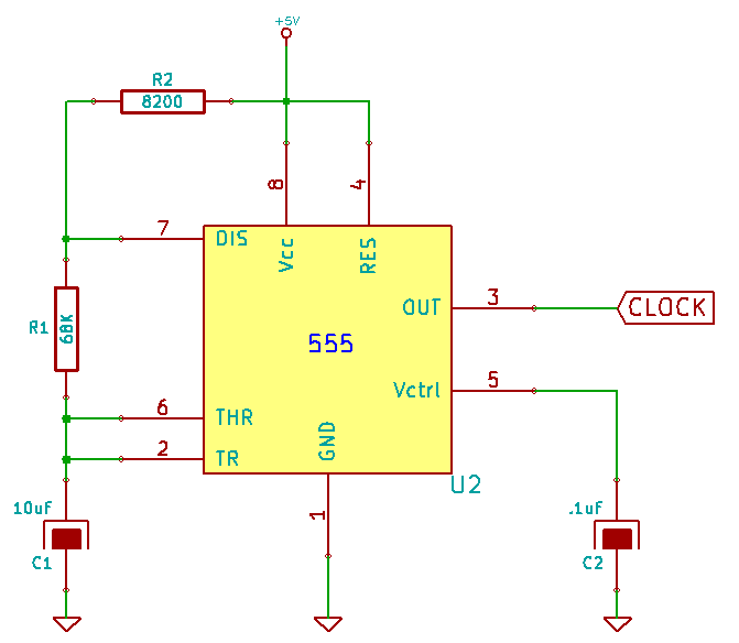
The values are chosen to generate a roughly 1Hz signal with a 50% duty cycle. A perfect 50% duty cycle is impossible with a 555 timer due to the different time constants generated by charging through two capacitors and discharging through one. It’s pretty close though, and certainly good enough for our purposes.
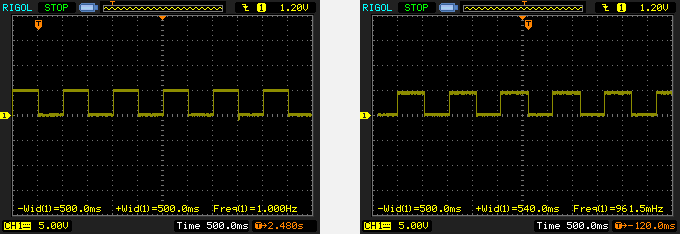
Here’s a comparison of the clock signal generated by the Arduino on the left, versus the 555 Timer on the right.
In part 4, we’ll look complete our understanding of signaling methods by creating a data signal as well.