In this module we’ll begin working with the AT25SF081 Flash Memory IC by readying individual bytes of data from the memory array.
Objectives
- Correctly create the SPISettings object.
- Determine which Memory Read opcode to use.
- Determine which which variable types to use for the address and data.
- Understand how to transmit the 24-bit memory address 8-bits at a time.
Background
AT25SF81 Functionality Overview Part 1
SPI Signals
Adesto AT25SF081 Datasheet
Schematic
Education Shield – AT25SF081 Flash Memory Subsystem
Setup
For this module, you’ll need the following equipment:
- I2C and SPI Education Shield or the AT25SF081 Flash Memory Breakout Board
- Arduino UNO R3
1. Mate the Education Shield with your Arduino UNO R3. If you’re using the AT25SF081 Flash Memory Breakout Board, connect 5V to 5V, 3V3 to 3.3V, GND to GND, HOLD to Digital09,CS to Digital10, MOSI to Digital11, MISO to Digital12, and CLK to Digital13. That’s a lot of pins!
2. Connect your Arduino to your USB cable, and use the Arduino IDE to upload the “Bare Minimum” sketch from the Basics section of the Examples.
Working with the HOLD pin is not necessary for any of the tutorials, it is only included on the breakout board for completeness. In the sketch it will always be set as an output in a high state, and on the I2C and SPI Education Shield, the pin is tied directly to the 3V3 rail on the PCB.
Reading AT25SF081 Memory
We’re going to start working with the flash memory using the read function, because this doesn’t affect the endurance of the NAND gates that make up the memory, so we can perfect our code without moving the chip towards the degradation point.
The individual bytes of memory are accessed using their 24 bit address, 0x000000 to 0x0FFFFF, and you can choose to start reading at any point in the array.
There are two read operations codes (opcodes), slow and fast. Slow Read, opcode 0x03, allows you to read the array up to a clock speed of 50Mhz. Fast Read, opcode 0x0B, allows you to read the array up to a clock speed of 80Mhz. The fastest clock speed the Arduino can achieve is 8Mhz, so either will suit our purposes.
For all work done on the AT25SF081, the opcode designating the action you want to take is the first item that is sent to the IC, after bringing CS low. To read data, you then send the 24 bit memory address associated with the byte you want to start with. If you choose to use the Fast Read command, you would then need to clock in a byte of junk data, for the Slow Read, this isn’t necessary.
After the correct read opcode has been issued (with the junk byte if necessary), data will begin to output on MISO, 8 bits at a time. As long as the clock keeps cycling, bytes of data will be read back in sequence indefinitely. If you reach the address at the end of the array, the internal pointer inside the AT25SF081 will move to the first address in the array, 0x000000, and start reading from there without you needing to take any action.
Once you’ve gathered as much data as you want, you bring CS high and that terminates the read operation.
SPISettings
We need to know three things to correctly configure the SPI settings for the AT25SF081. We need to know the speed at which it is capable of functioning, the bit order that data is transmitted in, and the SPI Data Modes the IC supports.
Page 33 of the datasheet shows that the slowest clock speed is associated with the 0x03 Slow Read opcode and is 50Mhz, so we can select the fastest Arduino clock speed of 8Mhz.
Page 6 of the datasheet states that all “data bytes are transferred with the most-significant bit (MSB) first.”
Finally, the same page of the datasheet says that the AT25SF081 supports SPI Modes 0 and 3 (0,0 and 1,1). This means that data is always sampled on the rising edge of the clock and latched on the falling edge, regardless of CPOL.
Combining these three items, we can build our SPISettings command as SPISettings AT25SF081(8000000, MSBFIRST, SPI_MODE0);
Declarations
As complicated as this chip is to work with (seriously, two modules to explain the functionality), there are surprisingly few things that need to appear in the declarations of our sketch in order to read data from the chip. We need to load the SPI library, establish the chip select pin (and the hold pin for the breakout board users), and define our two different read opcodes.
|
1 2 3 4 5 6 7 8 9 10 11 |
#include <SPI.h> // Include the SPI library SPISettings AT25SF081(8000000, MSBFIRST, SPI_MODE0); // Sets the pin values for the AT25SF081 and MCP3008 const int CS_AT25SF081 = 10; // Flash Memory Chip Select - Active Low const int holdPin = 9; // HOLD Pin - Active Low // Set bits for the various Flash IC OpCodes (see datasheet) const byte OPCODE_SLOWREAD_ARRAY = (0x03); // Memory read up <= 50Mhz (see datasheet) const byte OPCODE_FASTREAD_ARRAY = (0x0B); // Memory read up <= 85Mhz (see datasheet) |
Initialization
Because of the effects of chip endurance subsequent to 100,000 program / erase operations on the chip, and because these are educational modules and not production code, I am going to intentionally execute only small amounts of operations on the chip. One of the easiest ways to do this, is to ensure all chip operations occur within the Setup function, rather than the loop. This is a hamfisted way of preventing code from executing more than once, but it is effective.
The start of the Setup function is pretty cut and dried: we’ll prepare the Serial monitor and initialize the SPI bus, then set the pinMode for chip select (and Hold), and define the pin state.
|
1 2 3 4 5 6 7 8 9 10 11 |
Serial.begin(9600); SPI.begin(); // Set the pin modes pinMode (CS_AT25SF081, OUTPUT); pinMode (holdPin, OUTPUT); // Initialize the device for it's first interaction. digitalWrite (holdPin, HIGH); digitalWrite (CS_AT25SF081, LOW); digitalWrite (CS_AT25SF081, HIGH); |
After that basic stuff is accomplished, we’ll want to set the memory address we’re going to read. Addresses in the array are 24 bits in length, which means they exceed the space available within an integer variable type, two bytes, 0x2211. We need a larger variable type to hold our address value and the long type does nicely as it will hold three bytes of data, 0x332211. We can start anywhere in the array we want, and it would be perfectly ok to start at the beginning, 0x000000, but I’m going to select memory address 0x0FE8FF to start reading from, only so that it’s obvious on an oscilloscope when it gets transmitted.
|
1 |
long some24bitLocation = 0x0FE8FF; |
We’ll need a variable to hold the data returned from the flash memory, and we also want to go ahead and create our usual JUNK variable to send on MOSI, which generates clock cycles for data return.
|
1 2 |
byte memoryData = 0; byte JUNK = 0xFF; // Junk data for MOSI output |
Now we get into the meat of communicating with the chip. We’ll use our SPISettings object, bring CS low, and then send the Slow Read opcode. I’m choosing the Slow Read because Fast Read requires an extra byte of junk data to be transmitted before data is returned, which isn’t all that much of a performance hit at 80Mhz, but since we’re Arduino limited to 8Mhz, we may as well use the one that doesn’t require extra setup time.
|
1 2 3 |
SPI.beginTransaction (AT25SF081); digitalWrite (CS_AT25SF081, LOW); SPI.transfer (OPCODE_SLOWREAD_ARRAY); |
Sending the Memory Address
After the opcode is transmitted, we need to send our memory address. We have 28 bits to transmit (24 bits of actual address plus 8 leading zero bits), but each SPI.Transfer() command will only send 8 bits. That means we have to slice up the address into three sequenced chunks. We do this by masking off each byte of the memory address in turn, shifting that byte into the least significant position, then transmitting that result.
Data is transmitted MSB first, so we need to transmit the left most byte of address data to start with.

Remember, we only send eight bits, so if we just transmitted the masked data, we would only clock out the least significant eight bits, which are still just zero. That means we have to shift the values we care about into those least significant bit positions, 16 bits to the right.
|
1 |
(some24bitLocation & 0xFF0000) >> 16 |
For the middle byte of data, we perform a similar process. This time we mask off the middle byte of address value.

That middle byte is still 8 bits away from the LSB position, so we shift it over as well.
|
1 |
(some24bitLocation & 0x00FF00) >> 8 |
The last byte of address goes through a similar process. This isn’t entirely necessary, since the least significant byte is what would be transmitted by default, but I think it makes the code more clear, at the expense of a little efficiency.

|
1 |
(some24bitLocation & 0x0000FF) >> 0 |
|
1 2 3 |
SPI.transfer ((some24bitLocation & 0xFF0000) >> 16); // Byte address - MSB Sig Byte SPI.transfer ((some24bitLocation & 0x00FF00) >> 8); // Byte address - MID Sig Byte SPI.transfer ((some24bitLocation & 0x0000FF) >> 0); // Byte address - LSB Sig Byte |
Reading the Data
After the hoops you had to jump through to transmit the memory address, getting the data back is trivial. The chip will begin transmitting data on the next clock cycle after a valid address, and continue to do so until CS goes high again. Since we have to send data out on MOSI in order to generate the clock cycles, we’ll transmit our junk variable, and receive data back into the memoryData variable. After we receive our byte of data, we’ll bring chip select high again, release the SPI configuration and that is that.
|
1 2 3 |
memoryData = SPI.transfer(JUNK); digitalWrite (CS_AT25SF081, HIGH); SPI.endTransaction (AT25SF081); |
The Full Sketch
All that’s left to do is add some Serial Monitor output, formatted nicely for ease of reading. Once this is uploaded, you can open the serial monitor and you should receive a single line of output. Sort of anticlimactic, but a good start.
|
1 2 3 4 5 6 7 8 9 10 11 12 13 14 15 16 17 18 19 20 21 22 23 24 25 26 27 28 29 30 31 32 33 34 35 36 37 38 39 40 41 42 43 44 45 46 47 48 49 50 51 52 53 54 55 56 57 58 59 60 61 62 63 64 65 66 67 68 69 70 71 72 73 |
/* A sketch to control the 8-Mbit AT25SF081 Flash Memory IC. This sketch will read back a single byte of data from the memory address specified in the some24bitLocation variable within Setup. The code supposes the use of the Education Shield, but if you're using a breakout board, connect the CS pin to Digital 10, HOLD to Digital 9, and the SPI pins in their usual locations. Website: https://rheingoldheavy.com/at25sf081-tutorial-02-reading-memory-byte Datasheet: http://www.adestotech.com/wp-content/uploads/DS-AT25SF081_045.pdf */ #include <SPI.h> // Include the SPI library SPISettings AT25SF081(8000000, MSBFIRST, SPI_MODE0); // Sets the pin values for the AT25SF081 and MCP3008 const int CS_AT25SF081 = 10; // Flash Memory Chip Select - Active Low const int holdPin = 9; // HOLD Pin - Active Low // Set bits for the various Flash IC OpCodes (see datasheet) const byte OPCODE_SLOWREAD_ARRAY = (0x03); // Memory read up <= 50Mhz (see datasheet) const byte OPCODE_FASTREAD_ARRAY = (0x0B); // Memory read up <= 85Mhz (see datasheet) void setup() { Serial.begin(9600); SPI.begin(); // Set the pin modes pinMode (CS_AT25SF081, OUTPUT); pinMode (holdPin, OUTPUT); // Initialize the device for it's first interaction. digitalWrite (holdPin, HIGH); digitalWrite (CS_AT25SF081, LOW); digitalWrite (CS_AT25SF081, HIGH); long some24bitLocation = 0x0FE8FF; byte memoryData = 0; byte JUNK = 0xFF; // Junk data for MOSI output // Begin Reading Memory Over SPI SPI.beginTransaction (AT25SF081); digitalWrite (CS_AT25SF081, LOW); SPI.transfer (OPCODE_SLOWREAD_ARRAY); // Send OpCode SPI.transfer ((some24bitLocation & 0xFF0000) >> 16); // Byte address - MSB Sig Byte SPI.transfer ((some24bitLocation & 0x00FF00) >> 8); // Byte address - MID Sig Byte SPI.transfer ((some24bitLocation & 0x0000FF) >> 0); // Byte address - LSB Sig Byte memoryData = SPI.transfer(JUNK); // Read byte from address digitalWrite (CS_AT25SF081, HIGH); SPI.endTransaction (AT25SF081); // End Reading Memory Over SPI // Display the byte returned in the serial monitor with pretty formatting Serial.print ("Data in memory address 0x0"); Serial.print (some24bitLocation, HEX); Serial.print (": 0x"); Serial.println (memoryData, HEX); } void loop() { } |
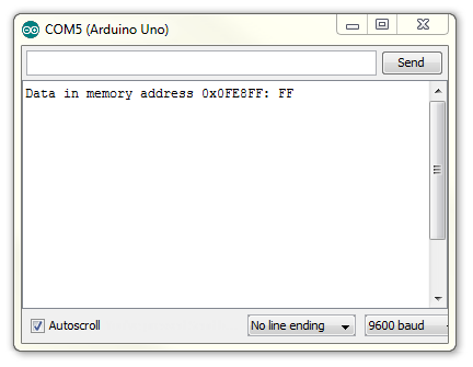
Remember, a byte is considered erased if all the bits are set to 1, so if you’re working with a new chip, you’re reading an erased byte of data, which is why the value returned in the serial monitor shows as 0xFF.
