In Part One we looked at individual logic gates. In Part Two we saw how to combine them to retain a single value. In Part Three we started making things synchronous by using a clock signal. Now we’ll explore adding data signals to our system.
Master Slave Flip Flop
Let’s finish up looking our exploration of flip flop types. I wanted to put this under the part 3, but that was already getting pretty long, so we’ll clean the subject up now.
When we first added a clock signal, we created level triggered flip flop, where SET or RESET are reflected at Q and NOT-Q the moment they are applied while CLOCK is high. Then we created an edge triggered flip flop, where input state is only sampled at the rising or falling edge of the CLOCK signal.
There is a third method, called “pulse” triggered. In this arrangement, SET or RESET are sampled while the clock is high as they are in the level triggered flip flop, but they are only applied to the outputs at the falling edge of the CLOCK signal.
The pulse triggered flip flop is called a “master-slave” flip flop, and it uses a whooooole mess of logic.
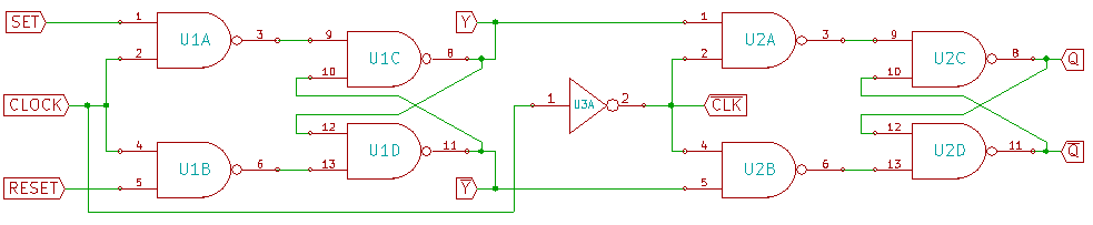
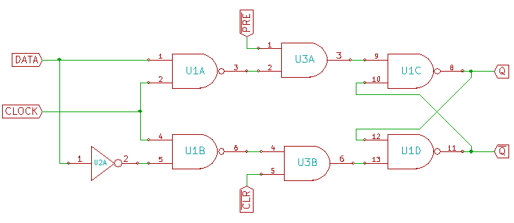
Essentially you have a pair of SR flip flops connected together. SET and RESET enter from the left as always, with the CLOCK entering as it did in part 3. At the boundary between the master and the slave, we will name the outputs Y and NOT-Y. They act as you would expect: SET = Y, RESET = NOT-Y. CLOCK, however, is passed through a NOT gate before it is used to trigger the slave flip flop. Consequently, the state will be held at the Y / NOT-Y point until CLOCK is brought low, engaging the second stage.! If you do the torturous logic, you’ll see how the second stage acts as a gatekeeper. That way, the value of the inputs is set to Y and NOT-Y when the CLOCK is high, but the state of the boundary area won’t be sent to the outputs until the CLOCK essentially shuts off.
As before, the green LEDs to the left represent SET, RESET and CLOCK, with red LEDs for the SET and RESET states. Now I’ve added yellow LEDs to represent Y and NOT-Y as well.
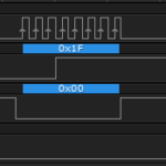
[masterslider id=38]Because the transition to high and back to low causes something to happen in the flip flop, any bouncing on your input CLOCK would cause whole a whole series of data points to be blasted through your flip flop. That’s why tactile buttons don’t really work here anymore.
You could add NOT and AND gates to the CLOCK to make the master positive edge triggered, that way you would only sample SET and RESET on the leading edge. Conceivably you could do so for the second stage as well.
A positive edge triggered master-slave flip flop is about as precise as you can make a single bit of data, and that is why this particular thing is so important.
JK Flip Flop
There is one last flip flop to mention, the JK type. In the JK (J=SET and K=RESET), the inputs are actually connected directly to the outputs, with the standard intermediary connections you would expect. The important thing to note about the JK, is that due to its configuration, it avoids the indeterminate state. When J and K are low, it is in a hold state. When J is high, it enters the SET state, Q. When K is high it enters the RESET state, NOT-Q. So far, sounds just like an SR flip flop. However, when J and K are both high, it doesn’t enter the indeterminate state, it simply toggles the output Q for NOT-Q or vice-versa. There is much to read on the subject of JK Flip Flops, and I think this page at Electronics Tutorials presents it very well.
Data Signals
We have one small problem remaining though for our flip flops: the indeterminate state. Throughout everything we’ve done so far: flip flops, SR flip flops, level triggering, edge triggering, pulse triggering, edge triggered master-slave flip flops, etc, we’ve always had to avoid the evil indeterminate state. We need to adjust things slightly so that we can eliminate it as a possibility.
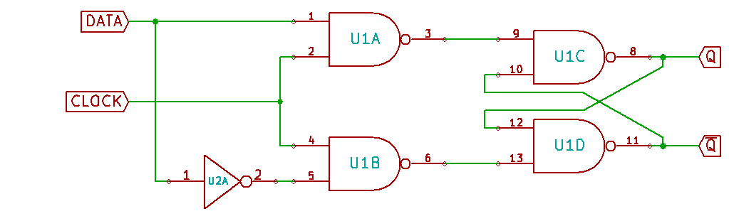
Take the SET signal, but instead of just sending it into the top NAND gate, use it as the input for the other NAND gate as well, but include an inverter before the bottom input. This way, SET and RESET will always be the opposite of each other! The single input is now called “DATA” and you’ve created a D-type Flip Flop!
As you can imagine, all the signalling tricks we worked with earlier can be applied to this beast, and you can easily transform it into an “edge triggered master-slave D-type flip flop.”
Symbolic Flip Flop Representation
Writing out all those gates gets to be unwieldy. For that edge triggered master-slave d-type flip flop, you would need to present 10 individual gates, just for one little BIT. There is a symbolic short hand for this that we can use to represent the flip flops in a more concise fashion.
The flip flop is represented as a vertical rectangle, with inputs on the left and outputs on the right. Bubbles are used to represent an inverted signal, as they did for the logic gates, but now we also add a triangle to represent edge triggering. Triangle alone = positive edge trigger, triangle with bubble = negative edge trigger. Here are some examples…
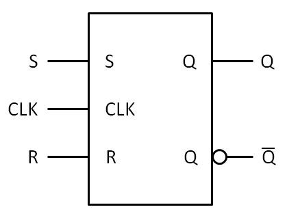
1. SR Flip Flop Symbol
This is a basic SR Flip Flop. You have SET and RESET on the left hand side, with a clock signal. There are no bubbles on the left, so nothing is inverted, and no triangles, so nothing is edge triggered. Our outputs are Q and NOT-Q, or Q and inverted Q, depending on how you want to read the symbol.
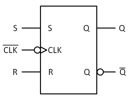
2. Negative Edge Triggered SR Flip Flop Symbol
This appears very similar to the one above. We have SET and RESET inputs on the left hand side, and Q and NOT-Q outputs on the right hand side. Our clock signal is different though, it is now edge triggered, represented by the triangle, and it is triggered on the negative going edge, represented by the bubble at the triangle.
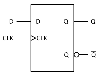
3. Positive Edge Triggered D Type Flip Flop
One final example. Now we’re looking at a D flip flop, as shown by the single DATA input on the left. It is edge triggered on the positive going side of the clock pulse, indicated by the triangle on the clock line (no bubble = positive edge). Our outputs are still Q and NOT-Q.
How sick are you of flip flops now?
Preset and Clear
It is common to add asynchronous controls to a flip flop, specifically “Preset”, to force the flip flop to a SET state, and “Clear” to force the flip flop into a RESET state. While the functioning of the data signal is synchronous, meaning it’s synchronized with the clock signal, PRESET and CLEAR are asynchronous as they occur outside of anything to do with the clock. They also override any values coming in on inputs. Typically, these inputs are active low, and you see them denoted that way with a bubble on their input symbolically, or with an overbar when included in the text of something like a datasheet.
The key to understanding how this works, is seeing that the flip flop array on the far right, is built with NAND gates, and if you remember from our original NAND gate Flip Flop in Part 2, the inputs are active low. That means, by holding PRESET low, you force the AND gate low putting the flip flop into SET. If you hold CLEAR low, you do the same thing, except forcing the RESET state.
Typically, you would see this in the datasheet for a logic gate array as a single SET or CLEAR or OUTPUT ENABLE input, that affects the entire array. You would also have to be careful to avoid bringing both PRE and CLR low, because you’ve just created the dreaded INDETERMINATE state.