This module continues developing our understanding of the AT25SF081 feature set. This module will cover the Status Registers, Security Registers and Data Protection functionality of the chip based on the datasheet. More hexadecimal comin’ at you!
Objectives
- Understand the purpose of the Security Registers.
- Understand the internals of the two Status Registers
- Understand the layers of data protection.
- Understand how to place the AT25SF081 into Deep Power Down.
- Learn the miscellaneous opcode commands.
Background
AT25SF081 Functionality Overview Part One
Decimal, Binary and Hexadecimal Number Systems
SPI Signals
How To Read A Datasheet
Adesto AT25SF081 Datasheet
Schematic
Education Shield – AT25SF081 Flash Memory Subsystem
Setup
There is no setup required for this module.
Security Register
There are three full 256 byte pages of isolated memory called the Security Register. These pages are independent of the main memory array, but are read, erased and programmed using the same techniques as listed in part one.
These sets of bytes are available to be used just as the other memory is, but have their own dedicated read/program/erase opcodes and can be locked from program and erase operations independently of the rest of the memory array. The idea is that you could put serial numbers, encryption keys, stuff like that in this area of memory, lock it off and not worry about it being accidentally overwritten by crappy code that overflows a page in the normal memory.
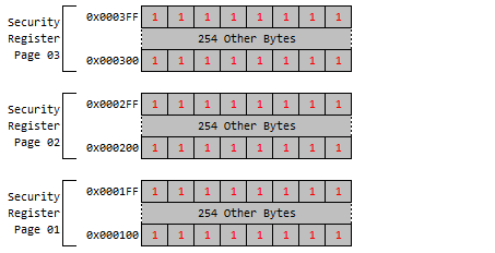
To read the security register, issue opcode 0x48 and follow the usual read methodology.
To program the security register, issue opcode 0x42 and follow the usual program methodology.
To erase the security register, issue opcode 0x44 and follow the usual erase methodology. When erasing the security register, you can only erase a full 256 byte page at a time, not more and not less.
Status Register
Data protection and device configuration all flow from the two bytes of the Status Register. The Status Register can be read, even when the device is busy programming or erasing memory, which is why you can poll the RDY/BSY bit to figure out when the device has completed a specific operation. Two different opcodes are used to read the Status Register, Byte 1 can be read using opcode 0x05, and Byte 2 can be read using opcode 0x35. Various opcodes are used to set the bits.
Status Register Byte 01
| Bit | Name | Description |
|---|---|---|
| 7 | SRP0 | Status Register Protection Bit 0 |
| 6 | SEC | Block Protection |
| 5 | TB | Top / Bottom Protection |
| 4 | BP2 | Block Protection Bit 2 |
| 3 | BP1 | Block Protection Bit 1 |
| 2 | BP0 | Block Protection Bit 0 |
| 1 | WEL | Write Enable Bit |
| 0 | RDY/BSY | Ready / Busy Status |
Status Register Byte 1 Bit 0 is the RDY/BSY bit – this bit displays the current operational status of the AT25SF081. If the device is free to execute read/program/erase commands, the bit will be cleared. If the device is currently chewing on some command already, then the bit will be set. This is done automatically by the chip itself and is read only. The Status Register can be continuously polled using the 0x05 opcode with a mask used to expose bit 0 to determine when the device has been freed up for further operations.
Status Register Byte 1 Bit 1 is the Write Enable bit – used to allow or disallow program or erase operations globally on the AT25SF081. The default state of this bit is 0 at power up, and is set using the Write Enable opcode 0x06. After the bit is set, it will be automatically cleared following the successful completion or intentional abort of an operation on the memory array, Status Register or Security Register. However, if the bit is set and the subsequent operation aborts because of an incomplete or incorrect opcode being sent, the bit will remain set until a correct memory array or Security Register program / erase command is received.
The Write Enable bit state is latched into the system on the rising edge of CS, so you must go through a full SPI cycle of bringing chip select low, clocking in the WEL opcode, and bringing chip select high again, before you can perform any program or erase commands.
Status Register Byte 1 Bit 2 is the Block Protection Bit 0 bit – determines the amount of the memory array protected from program / erase operations, and is set using the Write Status Register opcode 0x01 (see Data Protection section below).
Status Register Byte 1 Bit 3 is the Block Protection Bit 1 bit – determines the amount of the memory array protected from program / erase operations, and is set using the Write Status Register opcode 0x01 (see Data Protection section below).
Status Register Byte 1 Bit 4 is the Block Protection Bit 2 bit – determines the amount of the memory array protected from program / erase operations, and is set using the Write Status Register opcode 0x01 (see Data Protection section below).
Status Register Byte 1 Bit 5 is the Top/Bottom Protection bit – determines the amount of the memory array protected from program / erase operations, and is set using the Write Status Register opcode 0x01 (see Data Protection section below).
Status Register Byte 1 Bit 6 is the Block Protection bit – determines the amount of the memory array protected from program / erase operations, and is set using the Write Status Register opcode 0x01 (see Data Protection section below).
Status Register Byte 1 Bit 7 is the Status Register Protection Bit 0 – works in conjunction with SRP1 in Status Register Byte 02 to set the level of write protection covering the status register, and is set using the Write Status Register opcode 0x01 (see Data Protection section below).
Status Register Byte 02
| Bit | Name | Description |
|---|---|---|
| 7 | RESERVED | RESERVED FOR FUTURE USE |
| 6 | CMP | Complement Block Protection |
| 5 | LB3 | Security Register Page 3 Protection |
| 4 | LB2 | Security Register Page 2 Protection |
| 3 | LB1 | Security Register Page 1 Protection |
| 2 | RESERVED | RESERVED FOR FUTURE USE |
| 1 | QE | Quad Read Enable |
| 0 | SRP1 | Status Register Protection Bit 1 |
Status Register Byte 2 Bit 0 is the Status Register Protection Bit 1 – works in conjunction with SRP0 in Status Register Byte 01 to set the level of write protection covering the status register, and is set using the Write Status Register opcode 0x01 (see Data Protection section below).
Status Register Byte 2 Bit 1 is the Quad Read Enable bit – setting this bit converts the Write Protect and Hold pins of the AT25SF081 to output pins for use with the quad read opcode. This feature is unavailable on the I2C and SPI Education Shield and this bit should remain cleared.
Status Register Byte 2 Bit 2 is reserved by the manufacturer for future use. Attempts to set or clear this bit will be ignored.
Status Register Byte 2 Bit 3 is the Security Register Lock Bit 1 – it is used to lock Page 1 of the Security Register from program / erase operations. Security Register Page 1 addresses are 0x000100 – 0x0001FF.
Status Register Byte 2 Bit 4 is the Security Register Lock Bit 2 – it is used to lock Page 2 of the Security Register from program / erase operations. Security Register Page 2 addresses are 0x000200 – 0x0002FF.
Status Register Byte 2 Bit 5 is the Security Register Lock Bit 2 – it is used to lock Page 2 of the Security Register from program / erase operations. Security Register Page 3 addresses are 0x000300 – 0x0003FF.
Status Register Byte 2 Bit 6 is the Complement Block Protection bit – determines the amount of the memory array protected from program / erase operations, and is set using the Write Status Register opcode 0x01 (see Data Protection section below).
Status Register Byte 2 Bit 7 is reserved by the manufacturer for future use. Attempts to set or clear this bit will be ignored.
Data Protection
The first line of defense in protecting the data within the memory array is the Write Enable bit, the WEL bit, located in bit position 1 of the Status Register. To set the WEL bit, which allows program and erase operations, issue the opcode 0x06. To clear the WEL bit, which prevents program and erase operations, issue the opcode 0x04.
The Security Register is locked from program / erase operations on a per page basis using the LB3/2/1 bits in Status Register Byte 2.
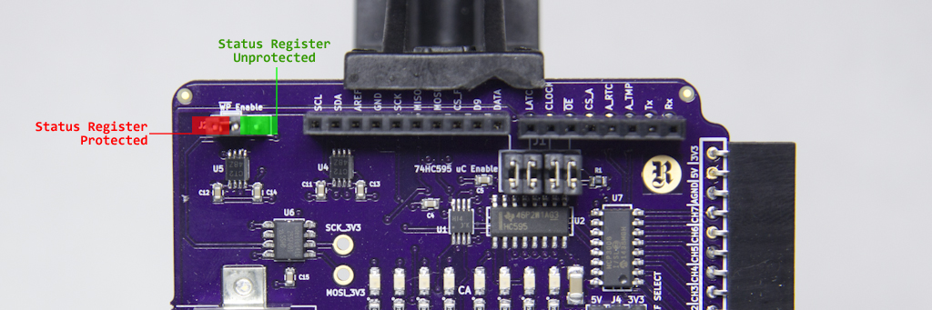
Further protection works in layers and is a little complicated. All protection of the memory array and the Security Register is governed by the state of the protection bits within the Status Register. If you can access the Status Register then you can change the security over all. Status Register access is managed using the Status Register Protection Bits 1 and 0, in conjunction with the Write Protect, WP, pin state, which is broken out to a jumper on the I2C and SPI Education Shield.
| SRP1 | SRP0 | WP Pin | Status Register Protection Level | Description |
|---|---|---|---|---|
| 0 | 0 | N/A | Software Level Protection | The only thing preventing writing to the Status Register is the state of the WEL bit. |
| 0 | 1 | 0 | Hardware Level Protection | The Status Register is locked and the bits are set as long as the WP pin is held at GND. |
| 0 | 1 | 1 | Hardware Level Protection Ready | The only thing preventing The only thing preventing writing to the Status Register is the state of the WEL bit. This will immediately be prevented as soon as the WP pin is held to GND. |
| 1 | 0 | N/A | Power On Reset Protection | The Status Register is protected from any modification until the next power down / power on cycle, when SRP1 will be cleared. |
| 1 | 1 | N/A | One Time Program | This will permanently fuse the current state of the Status Register and it can never be altered again. |
The first thing to note is at the bottom of the table: if you ever set both SRP0 and SRP1 simultaneously, you will instantly lock the state of the status register and you can never change it again. For the purposes of the Education Shield, it’s probably best just to leave the SRP1 bit cleared. SRP0 though, works with the state of the Write Protect pin that is broken out to a jumper on the Education Shield. If you set SRP0, then you allow the WP jumper to determine the protection state of the Status Register.
Now that you know how to protect the Status Register, let’s look at what you’re actually protecting.
The CMP, SEC, TB, BP2, BP1 and BP0 bits all work hand in hand to slice up the memory array into chunks of bytes that are protected from program / erase operations. In this way you can load the memory with some data that you don’t want modified, like alarm codes, tones or bit maps, and leave a section of the array open to being written for data logging or something like that.
Now I have tried to figure out what these bits mean, how they work, what their logic is, and I finally decided it’s a waste of time. You can’t protect an individual byte, only blocks of bytes, so pulling out the divining rod and attempting to decipher the hieroglyphics of that particular section of the datasheet is pointless. What you need to do is determine how many bytes you need to protect and whether you want those bytes protected from the bottom up, or from the top down, then use this chart to figure out how to set the six protection bits.
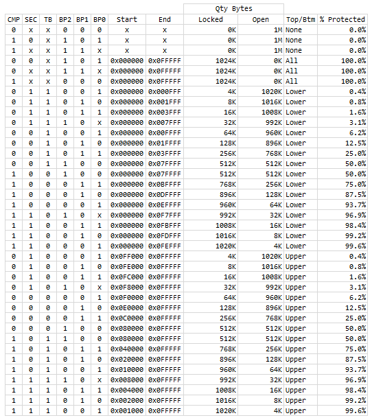
I know what a pain it is to see a graphic of a table, which can’t be sorted or copied, so here’s a CSV of the above data table… AT25SF081 Data Protection Bit Table.
For example, if you wanted to store the notes and tempo for the Mario Brothers Main Melody and the Mario Brothers Underworld Melody, you could take those 300 bytes of data (actually around 288 or so), and load them into the array starting at position 0x000000. The smallest amount of data you can protect is 4K bytes, so you may as well load up some other merry melodies to fill that space, then look at the chart and select how to protect the lower 4K of bytes.
All but the CMP bit are located in Status Register Byte 1, so are easy to set using a single Status Register Write command. The CMP bit seems to correlate with allowing you to protect more than 50% of the memory array at once, so if that’s how much data you need to protect, then you’ll need to set the CMP bit in Status Register Byte 2.
Setting Data Protection Bits
To set any of the data protection bits, you must first set the WEL bit. With WEL = 1, follow up with the Write Status Register opcode 0x01. When that command is issued, you can choose to send one byte or two bytes, which will write to Status Register Byte 1 and Status Register Byte 2 in turn, but sending byte 2 is completely optional.
The Status Registers are non-volatile (NV), just like the rest of the memory array, and are subject to the same endurance limitations. On device power-up, the contents of the NV Status Registers is copied to a volatile version as well (just like the power up process of the AT30TS750A). You can choose to make your changes to the volatile Status Register if you so choose, by issuing the “pre” opcode of 0x50. You would set the WEL bit, issue the pre-opcode, then issue the Write Status Register opcode, and your bits will be redirected to and from the volatile version, for that one command only. Each time you want to manipulate the volatile register, you must issue the pre-opcode.
Deep Power Down
By issuing opcode 0xB9, you can place the device in a deep power down mode, provided the RDY/BSY bit allows operations. In deep power down, the AT25SF081 will draw only around 2µA of current as opposed to the 13-25µA of current it would draw while just sitting there remembering things. As it can get pretty current hungry, 10-16mA current draw for all program and erase functions, it can be very beneficial to go into deep power down if you’re running off a battery. From CS going high after issuing the opcode to the device entering deep power down mode requires only 1µs.
Once in deep power down, the only opcode that will be recognized by the chip is Resume From Deep Power Down, 0xAB. After the Resume opcode is issued, the chip to a fully standby ready state within 5µs of CS having gone high .
Other Miscellaneous Hoop Jumping
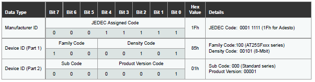
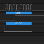
There are manufacturer and device IDs hardcoded into the chip that can be read using the opcode 0x9F. Issuing this opcode will return three bytes of data, one byte of MFG ID that should equal 0x1F, and two bytes of Device ID that should equal 0x85 and 0x01 respectively. These values are set at the manufacturer and are read only. They correspond to the values displayed in the datasheet which I am too lazy to do anything but capture a screen capture of at this point…

