This module provides detail on the SPI signals, including the different clock polarities and phases.
Objectives
- Understand the differences between the clock polarities
- Understand the differences between the clock phases
- Learn how to define the clock polarities and phases as SPI Modes
- Determine if SPI is an MSB or LSB first technology
- Understand how the configuration freedom may cause errors
Background
SPI Basics
Reading through the previous sections will be helpful for the less experienced, but are not necessarily essential.
Schematic
No schematic is associated with this module.
Setup
This module is dedicated to SPI theory, so no hardware is necessary at this point.
SPI Signals
SPI has no standard defined for it. Nothing states that all day must be sent on the leading edge and data transitions occur when the clock is low, as is made clear in the I2C standard. You pulse the clock and data is sent and received simultaneously, however you have to specify yourself when data is considered valid and when data can transition states. More so than in I2C, understanding edge transitions becomes important when deciphering SPI signals.

With SPI, you’re governing an interaction with a series of shift registers. The MOSI line is used to shift data into a register located within the slave component, MISO is used to shift data out. Remembering the interactions you had with the shift register subsystem on the I2C and SPI Education Shield, you can think of MOSI and MISO as the data signals, and the CLK line is synchronized in direct opposition with the LATCH — when CLK is high, LATCH is low. In this way, you move data constantly through the shift registers. Looking at the SPI half of the diagram above, every time the column is green, new values are latched from the shift registers and made available on the data lines, then every time the column is red, the states of those lines are sampled, and data is thus recorded.
SPI Modes
It can be confusing that it isn’t set it stone if the clock starts high and latch starts low or the other way around, or even if data is sampled on the rising or falling edge of the clock pulse. These are all configurable as the two halves of the SPI Mode: Clock Polarity and Clock Phase.
Clock Polarity
Clock polarity dictates whether the clock idles in a default logic high or logic low. (There are two different types of chips on the Education Shield and one of them is 5V and the other is 3V3, so in each case, a valid logic high is interpreted as 70% of the respective VSUPPLY.) Clock Polarity is commonly abbreviated as CPOL, with CPOL = 0 meaning idle at logic low and CPOL = 1 meaning idle at logic high.
Clock Phase
Clock phase dictates whether the latch is triggered first or sampling is triggered first. The latch would be considered to occur on the opposite edge of the same clock pulse. Even though the latch is internal to the silicon guts of the chips involved, it is occurring. If you ever read about SPI data being “shifted” or “toggled”, as opposed to sampled, they are referring to the internal latching mechanism. Pay attention though, that the phase configuration only determines which goes first: trigger or sample, not if it happens on the rising or falling edge — that is determined in combination with the CPOL. Clock Phase is commonly abbreviated as CPHA, with CPHA = 0 meaning sampling occurs on the rising clock edge and CPHA = 1 meaning sampling occurs on the falling clock edge.
For more detail on the concept of edge triggering clock signals, please refer back to the Clock Signals module in the Digital Logic Basics section.
SPI Modes
The CPOL and CPHA values are combined to form the two bits of the SPI mode, resulting in a decimal value of 0 to 3.
| Mode Value | CPOL | CPHA | Clock Idle Status | Clock Latch and Sampling Phase |
|---|---|---|---|---|
| 0 | 0 | 0 | Clock Idles Low | Sample on the initial clock edge, latch on the subsequent edge. |
| 1 | 0 | 1 | Clock Idles Low | Latch on the initial clock edge, sample on the subsequent edge. |
| 2 | 1 | 0 | Clock Idles High | Sample on the initial clock edge, latch on the subsequent edge. |
| 3 | 1 | 1 | Clock Idles High | Latch on the initial clock edge, sample on the subsequent edge. |
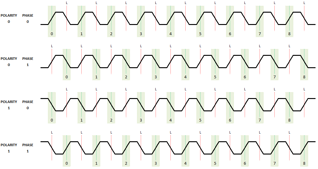
The good thing to know about the various SPI modes, is that you just have to dig into the datasheet for your particular component to find out what modes it supports, and then use that one. Further, 90% of the time you’ll discover that the chips support MODE0 and MODE3, because in both of those instances, as you can see in the mode diagram above, the data is sampled on the rising edge of the clock pulse.
Deciphering SPI Data
The Arduino (and the underlying Atmel microcontroller at it’s heart) always processes SPI data 8 bits at a time, so if the data sizes you’re dealing with are greater than 8 bits, you’ll need to handle it appropriately. The bit order, Least Significant Bit First or Most Significant Bit First is also a configurable item in SPI. Fortunately, this particular configuration is also dealt with explicitly in each datasheet you’ll work with.
However, this means that for every chip that’s out there, you’ll need to know the correct bit order, clock polarity and clock phase associated with it. And if your SPI bus has chips on it that use different specifications, you’ll need to constantly reconfigure your SPI bus prior to every interaction with those devices, which causes overhead.
Further, the lack of an ACK/NACK signal, as there is in I2C, means that it’s up to you to determine if the data you’re receiving is correctly formatted, correctly obtained, or even if the chip you’re trying to interact with exists. How do you know that the value you’re requesting from the chip is actually 0x00 or if the chip has a bad solder connection on MISO?
Here is the Manufacturers ID value returned from the AT25SF081 Flash RAM module on the Education Shield, using each permutation of the possible configurations…
| SPI Mode | Bit Order | Output Value |
|---|---|---|
| MODE0 | MSBFIRST | 0x1F |
| MODE0 | LSBFIRST | 0x00 |
| MODE1 | MSBFIRST | 0x00 |
| MODE1 | LSBFIRST | 0x00 |
| MODE2 | MSBFIRST | 0x0F |
| MODE2 | LSBFIRST | 0x00 |
| MODE3 | MSBFIRST | 0x1F |
| MODE3 | LSBFIRST | 0x00 |
Three possible values result, but without reading the datasheet, there would be no way to determine which is the valid response. We’ll use checks like this going forward to verify data that we’re receiving over our SPI bus.
