One of the fastest ways to troubleshoot an I2C bus problem, is to pull up the signal on an oscilloscope and see if the system is doing something that matches your expectations. We’re going to turn that slightly on its head by taking a scope trace and using it to reverse engineer the I2C signal data from it.
Objectives
- Understand how to read an oscilloscope screen
- Identify the free state, start condition and stop condition
- Determine the I2C address of the slave component
- Determine the data direction by determining the R/W flag
- Find the ACK and/or NACK signals
- Determine the value in binary and hex of the data being returned
Background
I2C Basics
I2C Signals
Schematic
No schematic is associated with this module.
Setup
The goal of this module is to focus on the signal itself, rather than on the hardware, however this module can be replicated in its methods by using any two channel oscilloscope capable of reading a 100kHz signal connected to the SDA and SCL lines between an Arduino and any I2C chip.
I2C Signal Reverse Engineering
We are going to take an oscilloscope trace and pull it apart to find all the various I2C values and parameters that are being sent back and forth between the Arduino and the slave component as shown in the I2C Signals module. We’ll make note of their values for use at the end, as we pull them out of the soup.
So first, let’s have a look at the overview of the whole signal.
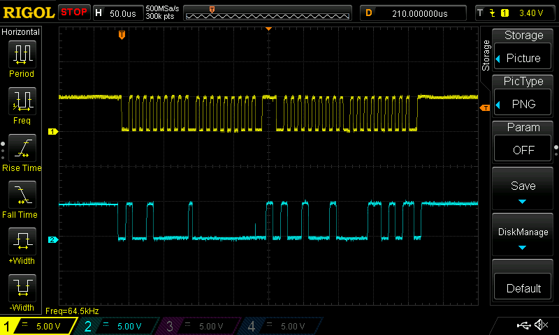
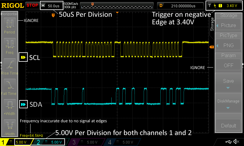
The first thing we note, looking at this, is that four bytes of data are being sent. We can’t tell which direction they’re going yet without pulling the strands apart though. The scope settings are 5V per division on the vertical scale and 50µS per division on the horizontal scale. The 5V lets us see pretty clearly each state change of the signals, and the time scale lets me fit the entire four byte conversation into one window.
I2C Signal Reverse Engineering: Byte 01 Detail
So let’s zoom in on the first byte. We are expecting to see the free state and start condition to begin with, then address bytes followed by a R/W bit followed by the ACK/NACK.
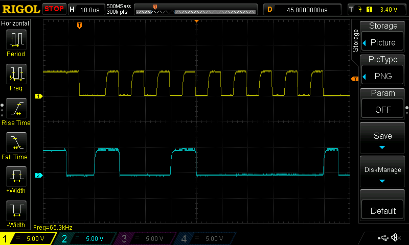
Before I slice it apart, make a note of something else. Do you see how there is a hint of a gentle slope to the positive going edge? That’s due to the bus capacitance and is showing you that the bus doesn’t just go smack straight to 5V, but has a slight charging curve to it because of CBUS as described in the I2C Pull Up Resistor module.
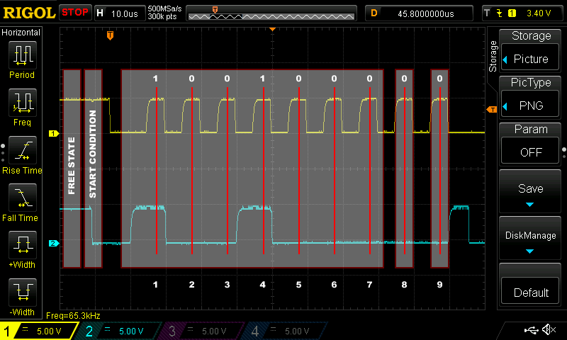
At the far left, you can see that the free state has been established as both the SCL and SDA lines are at 5V, and have been at 5V for a period of time that’s simply not seen on the trace.
This is followed by the start condition: the master pulls the SDA line low while keeping the SCL line high, letting the slave component know that something’s about to happen: address transmission.
The 7-bit address gets pulsed out and you can see it translates to a binary value of B1001000 or 0x48.
The next bit is the R/W flag and since it’s logic low, that means a WRITE… the master will be sending data.
The next bit is the ACK/NACK bit, and since an ACK is confirmed by a logic low on the SDA line, the slave component that corresponds to I2C address 0x48 is saying “I confirm I got the address and it’s mine… bring it on big guy!”
When looking at the detail of the scope trace, also note that the SDA bus doesn’t change state when the SCL line is high. First, the SCL line has to drop to GND, then the SDA line can change if it has to. The delay is only a few nanoseconds, which isn’t much, but it’s definitely NOT simultaneous. Remember that the SDA line must be in a stable state throughout the entire SCL logical high. It is only allowed to transition between states when SCL is low, otherwise you’d be trying to establish a start / stop condition.
Summary: The I2C master has told slave component 0x48 to expect data and the slave component said OK.
I2C Signal Reverse Engineering: Byte 02 Detail
Here is the second byte, without my graphic overlay. What you should expect to see in this byte, is 8 bits of data and then either an ACK or a NACK.
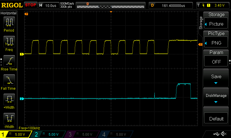
And here it is with the overlay…
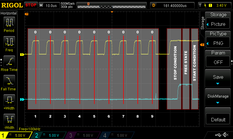
You might first look at that and thing, “Oh hell, something must be wrong!”. Well, no. Trust the fact that maybe you are supposed to be seeing a whole bunch of zeros.
For the data transmission, there are 8-bits, and the value of that data in binary is B00000000 and in hexadecimal it’s 0x00.
Bit 9 is the ACK/NACK bit and is a logic low as well, so the slave component is once again acknowledging that it successfully received the data.
At the very end, the master creates the Stop Condition, we enter the Free State for a bare fraction of a second and immediately we enter the Start Condition again, which will be the beginning of the third byte.
Summary: The master transmitted the value 0x00 which the slave acknowledged.
I2C Signal Reverse Engineering: Byte 03 Detail
Here is the third byte without the overlay. We know there is Start Condition, so we’re expecting to see a 7-bit address transmitted, a R/W bit and an ACK/NACK again.
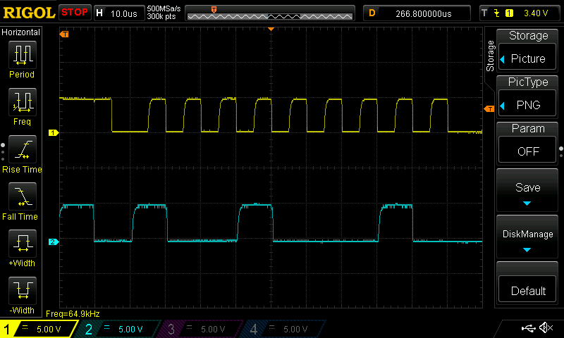
And here it is with the overlay…
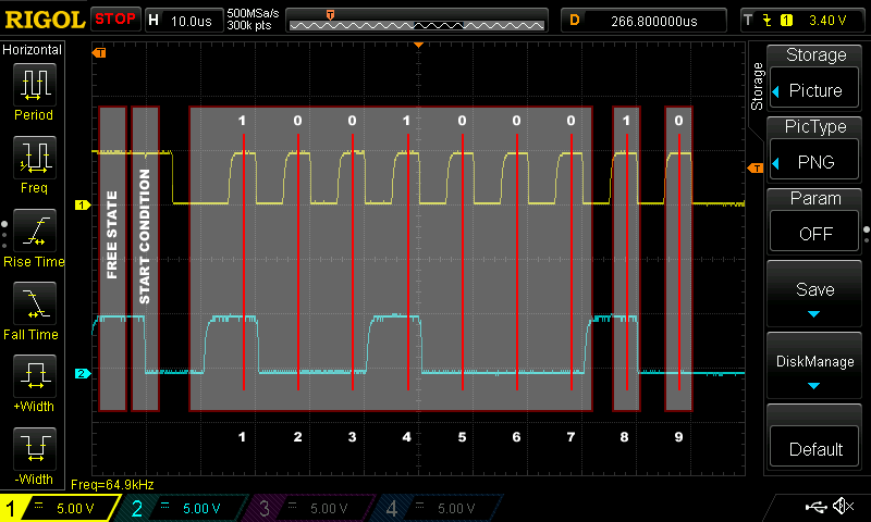
As we saw at the far right of the previous byte, the Start Condition is created by the master, by dropping SDA with SCL held high as well.
The SCL line then starts ticking away and we see the 7-bit address transmitted again on the first seven clock cycles, corresponding to binary address B1001000 or 0x48 in hex, which is the same I2C address that we sent in byte 01 above.
The R/W bit comes next, and is a logic high, meaning that the master is telling the slave component to transmit a byte of data next.
Finally, on bit 9, the slave sends an ACK by holding the SDA line low.
Summary: The I2C master has told slave component 0x48 to send data and the slave component said OK.
I2C Signal Reverse Engineering: Byte 04 Detail
The fourth byte without the overlay. As we’ve just sent the address, expressed the direction we wanted data to go and received an acknowledgement, we are now going to get back 8 bits of data with an ACK/NACK. If it’s an ACK, we’d expect a repeat start condition as before, if it’s a NACK, that is the master confirming that the slave can stop, and we would expect a full stop with a return to the free state.
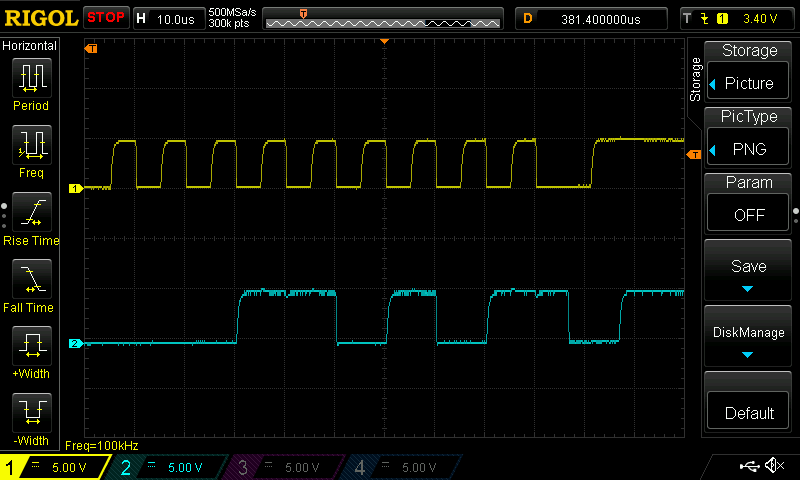
And here is byte 04 with the detail overlay…
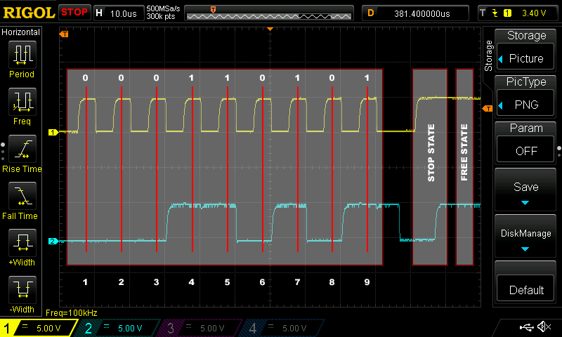
As with byte 02 above, the first eight clock cycles are all data, in this case, instead of a bunch of zeros, we’re getting some variation. The data evaluates to B00011010 in binary or in hex, 0x1A.
Then we receive a NACK in the ninth bit. That means the master is saying “got the data”.
The master then creates a stop condition by very deliberately, bringing the SDA line low, so it can bring the SCL line high, so that it can bring the SDA line high with the SCL line high, which is the definition of the stop condition.
Finally, it holds this long enough to enter the free state.
Summary: The master receives the value B00011010 or 0x1A from the slave, sends a NACK to end the conversation, manufactures the stop condition and allows the I2C bus to enter the free state.
I2C Signal Reverse Engineering Results
Here’s what we just saw…
- The Arduino told slave 0x48 to expect some data
- The Arduino sent the value 0x00 to slave 0x48
- The Arduino told slave 0x48 to send some data
- The Arduino received the value 0x1A from the slave and closed the line after one byte
This entire sequence, is how the Arduino requests and then reads the temperature reading from the AT30TS750 temperature sensor on the I2C and SPI Education Shield.
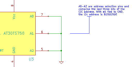
First it sends the address 0x48. In the datasheet, it shows that the I2C address is configurable for the AT30TS750, with three pins dictating the values of the three LSB of the 7 bit address, depending on their voltage level. In the design, I pulled all three pins to ground, so the LSB of the address would be 000. The data sheet also says that the four MSB of the address are fixed at the factory as 1001. So when you put the full address together you get B1001000 or 0x48. The Arduino then says that it is going to send some data.
Second, the value 0x00 is sent to the temperature sensor. In the datasheet it says that you need to tell the device which register you’re going to interact with. Registers are memory structures inside the chip created by digital logic, and we’re telling the device that we want to interact with the data at memory location 0x00. According to the data sheet 0x00 corresponds with the “Temperature Register”, or the memory location in the chip where it stores the current temperature reading. The chip is now set to blast back the temperature listed in its buffer the next time it has it’s address sent.
Third, you know what’s happening: 0x48 is addressed again, but this time the master is saying, “send me the current temperature”, with the AT30TS750 acknowledging.
Fourth and finally, the temperature sensor sends the value 0x1A, after which the master closes the conversation with a NACK and a stop condition.
0x1A is decimal value 26, which is the temperature in degrees centigrade in the lab, or around 78 degrees Fahrenheit. It’s a warm January here in Los Angeles in 2015.
