I’ve been wondering what might be interesting as a series to write, that would help people to understand what this world of makers is that we live in, what the possibilities are, and what one can now accomplish with a little forethought and attention to detail. I wanted to cover a topic that touched on many bases, from design to fabrication to thought process, but still was grounded in a subject that was approachable be even the majority of beginners.
So I decided to build an Arduino from scratch.
Update: here is a link to the full series: Build An Arduino UNO R3 from Scratch Table of Contents
I think this is an interesting project because it involves doing something I don’t usually do: take someone else’s design and attempt to replicate it. I have four things to use as a reference for this…
- The official open source schematic published by arduino.cc
- The official way the pins and connections are laid out for shield compatibility
- An actual official Arduino UNO R3 here to use for comparison
- The firmware published by arduino.cc
Beyond that, the selection of components, the manner in which they are arranged, the design considerations that must be addressed, the research in what the subsystems are, how they work, how they interconnect and how they need to be laid out, is all on me. I’ll need to pull up datasheets to verify assumptions made from reading the schematic, too and once the board is ready for fabrication, I’ll also start digging into the firmware.
In the end, I’ll publish a full set of KiCad design files, production Gerbers that can be uploaded to OSHPark, and a BOM with all the components valid as of the time of production (not sure if I’ll maintain it long term, but we’ll see). I’ll also write all the steps necessary to go from a board with a pile of components in the shrink wrap (or cut tape as the case may be), to a fully functional Arduino. In this way, hopefully others will be able to learn and play with the files and hopefully be able to build their own Arduino UNO R3 clone.
The Arduino UNO R3 Schematic
Because the Arduino is an open source hardware design, arduino.cc publishes the current schematic and is available at this link: Arduino UNO R3 Schematic
Soooo… great. Got a schematic. Now what do you do with it?
I think the first thing I’ll want to do is try to identify some of the major subsystems. I know there’s a DC connector on there, so there will be some manner of voltage regulation. There’s a USB connector, so some USB/Serial thing will be on there. Of course there’s the microcontroller (henceforth referred to as the uC) as well.
I think printing this thing out, dead tree style, is probably a good way to go. I am incredibly grateful to arduino.cc for making these schematics public, but let us be real, these aren’t the easiest things to read. A lot of the reference designators (“R3”, “C1”, etc) are overwritten by part numbers, as are the interconnections themselves. I’m sure it would be a bit easier to read if it were color coded, or broken into hierarchical sheets. I’ll remember to do that when I get to the point of drawing my own schematic.
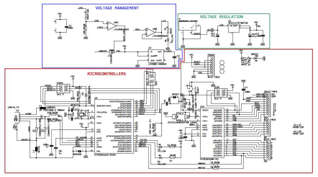
Looking at the printout, there are three obvious subsections. There’s the power input from the 9V jack with voltage regulation. There’s the voltage management section, which prevents voltage from being sourced from USB and the 9V jack simultaneously. There’s the uC section, comprised of two uC’s.
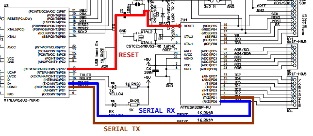
Going a little deeper, I want to see what the interconnection points are between the systems, besides power and ground — what signals are being communicated. It turns out there are only three signals shared in common between the two uC’s. Reset/Pin1 on the 328P is connected to Pin13/PORTD7 on the 16U2, Serial Rx/Pin2/PORTD0 on the 328P is connected to Serial Tx/Pin8/PORTD3 on the 16U2, and Serial Tx/Pin3/PORTD1 on the 328P is connected to Serial Rx/Pin8/PORTD2 on the 16U2. That’s it.
So, that means the uC section really breaks down into the USB-to-Serial interface controlled by the ATMEGA16U2, and the actual Arduino Brain ATMEGA328P-PU, that is the thing that we all think of as “Arduino”.
Arduino UNO Schematic R3 Fiddly Bits
Other things to note on the schematic that are maybe unusual for those that don’t look at these things day in and day out…
Resistor Networks
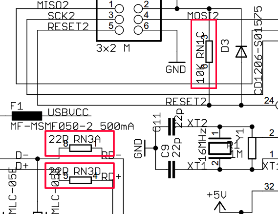
Most of the resistors on the schematic are listed as “RN#” followed by a letter. These are “Resistor Networks”, meaning a whole bunch of individual resistors bundled into a single package. The “#” is the reference designator, just like R1, R2, except RN1 and RN2, and the letter afterwards indicates which individual resistor in the package is being used.
Capacitor Values
A few of the capacitors on the board are listed in nano-farad values, which is 10-9. It looks like most of those are 100nF, which is a 0.1uF capacitor, and most of those are being used as bypass capacitors.
Static Discharge (ESD) Protection
There are a pair of varistors on the schematic, but they have a semi-unusual symbol that you might not run into very often… sort of a box with a slash through it. Those little guys have a super high resistance at normal voltage levels, but if you plug in a USB cable with a high static charge (or you have a high static charge from walking on a carpet before plugging in the cable), their resistance drops dramatically, providing a safe discharge path for the transient voltage spike caused by static electricity.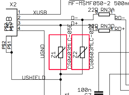
In part 2, I’ll start digging into voltage regulation subsystem.
