This module begins our discussion of SPI basics by introducing the theory, structure and signalling of the SPI serial communications bus. This is just an overview, with the most important aspects receiving their own dedicated modules to provide greater detail.
Objectives
- Understand what SPI stands for.
- Understand how components on the SPI bus are connected.
- Understand why pull up resistors are not needed.
- Define the four signaling lines in a SPI system.
- Determine how SPI components are selected for communication.
Background
This is the first module describing SPI, consequently, reading through the previous sections will be helpful for the less experienced, but are not necessarily essential. Here are some additional resources for those interested in obtaining greater technical detail…
Schematic
No schematic is associated with this module.
Setup
This module is dedicated to SPI basics theory, so no hardware is necessary at this point.
SPI Origins
SPI stands for Serial Peripheral Interface and was developed by Motorola. It was introduced in 1985 for use with the M68HC11 microcontroller. The Arduino has an internal subsystem dedicated to managing SPI interactions and has four pins dedicated to this functionality, although you’ll only likely use three of them for the most part. The name, “SPI” is pronounced commonly by either it’s individual letters, “S. P. I.”, or as an acronym pronounced like “spy”. (My brain flips between the two at will, so I apologize in advance for sentences that read “…many devices can exist on a SPI bus, however we’ll want to have an SPI bus that…”)
The SPI standard, such as it is, is much looser than that for I2C, and manufacturers are able to develop their signaling schemes using a wide variety of speeds and triggering methods. The SPI system is accessed using the SPI library, and is capable of running at seven different speeds, from 62.5kHz up to 8mHz.
All SPI chips are managed in a single master model, meaning only one device on a SPI bus will ever control the clock signal. A chip is told that communications are going to begin with it by pulling a specific pin to a logic low state. There is no addressing signal mechanism necessary in SPI as there is in I2C.
SPI has the added benefit of having individual datalines for each direction of communication, this allows bidirectional simultaneous data transfer between the master and the secondary component.
SPI Hardware Details
SCK, MISO, MOSI, SS
Every SPI implementation will include three signaling lines at a minimum: the clock line called SCK, the Master In / Slave Out line called MISO (Me-So) and the Master Out / Slave In line called MOSI (Moh-See). In addition to these three lines, you will most commonly have a Slave Select line, SS, that governs which chip is being controlled at any particular time. This line can also be referred to as “Chip Select” and is always active low. The SS line on the Arduino is the Slave Select line for the ATmega328P, and would be used if the Arduino was acting as a slave on the SPI bus, however the SPI library does not support that activity.
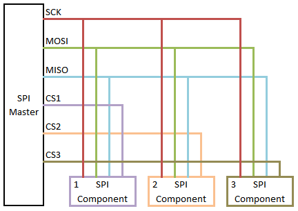
Typically, the three primary pins of the SPI system, SCK, MISO and MOSI, will be connected in a bus fashion, each tapping into the line at some point along the way. In rare instances though, chips can be daisy chained together with the MISO pin of one chip connected to the MOSI pin of the next chip in order, with SCK and CS connected bus fashion. In this way, all the SPI devices are activated at the same time with CS going low, and data is clocked through the system from one chip to the next. This architecture won’t be covered in these modules, but more information about this configuration can be found in this Maxim Integrated AppNote: Daisy Chaining SPI Devices.
Amount of Devices
There is no specified limit to the amount of SPI devices that can exist on an SPI bus. Practically though, every SPI chip that your microcontroller will want to interact with, will need to have a signal line routed to it to manage it’s chip select pin. The limited availability of GPIO pins on your micro and the complication of routing those signal traces on a PCB impose a physical limit on the amount of devices, if not a logical one.
Push/Pull vs. Open Drain
In general, there is no need for pull up resistors in a SPI implementation, because the pins use a push-pull configuration, rather than Open Drain. The output pins are capable of actively creating their own logical high and low states, rather than relying on pull up resistors to generate a default state. The diagram below represents the classic push-pull configuration using transistors, however invariably this is now implemented with CMOS technology.
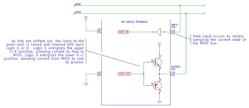
There are unique instances where pull up resistors are necessary, in order to provide a specified state for one of the buses. For example, SD card readers tend to begin as I2C devices at powerup and are then configured during chip initialization to communicate over SPI. If the I2C and SPI systems share the clock and data bus, then RPU would be a necessary component in that design. As with every single thing in electronics, careful reading of the datasheet will guide you.
Addressing
As there is no address that needs to be transmitted on the bus to indicate which device is being chosen for interaction, you can have multiple identical chips on the bus without worrying about communications conflict. If you want to pick a chip to speak with, just bring it’s chip select pin low and hammer away.
SPI Basics: Signaling Details
The signaling in a SPI implementation is essentially very simple, however due to the lack of an established signalling standard, there are various “SPI Modes” that the system may need to carry. These modes govern the polarity of the clock signal, and the edges on which data is sent and received. This will be covered in greater detail in the next module.
At it’s essence, the master device will indicate which component it wants to work with by pulling that chips corresponding Chip Select pin low. CS is always active low.
After CS is brought low, the master begins to clock out pulses on SCK. What happens at this point is dictated by the chip with which you’re communicating. As the SPI bus is bidirectional, data may be present on either, or both, MOSI or MISO on that first clock pulse, and it is up to your code to handle the transmission or reception of data appropriately. In some cases, you will be expecting to simply receive data, in some cases you’ll expect to only send data, in some cases, you’ll be expecting to send data at the beginning of a byte transfer and be receiving data by the end of it.
The MISO and MOSI sections of a chip act as shift registers, clocking data in or out as the SCK signal is received, and one of the primary features of SPI, is that they are able to do so simultaneously. This will continue as long as CS is low and the clock stays active.
SPI data can be sent either LSB or MSB first, and that information is contained in the datasheet for the components you’ll use.
