The phrase “failing fast” is commonly associated with software. With hardware, short of paying a huge premium for quick turns on board fab, you simply have to wait, generally weeks on my budget, to receive boards to test. That timeline is causing stress on my business, so I’ve looked for other solutions. Enter The Othermill.
The Problem with Time
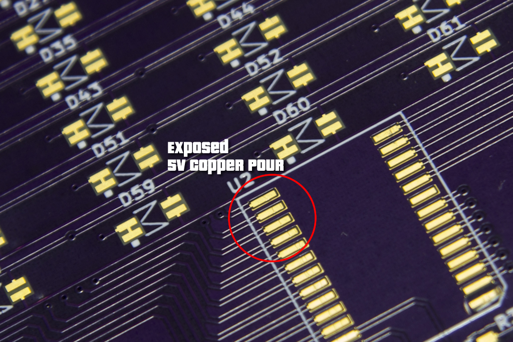
There was a moment when I realized that I was no longer making PCBs for fun, but for a living. I remember it very well, because it came not after the sale of something I had designed, but on the heels of a mistake. I received a board from OSHPark and it had an absolutely fatal and glaring flaw. I didn’t know that upgrading KiCad would result in an increase in the default exposure of soldermask relief on my board from 0.002 inches to 0.006 inches. That exposed the power plane around each and every pad, around each and every IC on the board. TL/DR: The whole board was shorted to 5V.
Previously, my attitude towards this was that it wasn’t much of an issue: money lost on parts and money lost to respinning the board, but I can get money from selling more boards. What I could not do, what I cannot recreate, is the time lost to getting that board respun.
The initial design was started in June of 2015… the first board was ordered in August, three weeks later it arrived, but there was a problem with some coating on the board preventing solder from adhering, so three weeks became six weeks. Then I discovered the problem with the short circuit. Nine weeks into it, and I hadn’t tested a single aspect of the design yet. That’s over two months!
That’s when I started thinking about how to decrease the length of time it takes me to go from idea to design to proof of concept to prototype to production.
Othermill
The Othermill (https://othermachine.co) is a desktop milling machine. A tiny little cutting bit, in a very precisely controlled machine, isolates your traces and pads out of a sea of copper on a slice of FR1. The primary benefit is that it allows you to iterate those designs in a matter of hours, instead of weeks. There are compromises of course: low resolution design constraints, lack of plated vias and a lack of soldermask.
Plated Vias
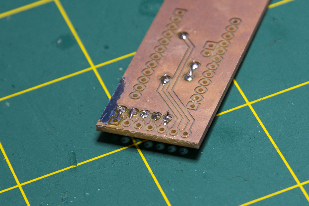
We’ll talk about iterating our designs in a moment, but let’s quickly talk about the compromises. Firstly, you can’t get plated vias. This makes sense because even if you’re using a PCB blank with copper on both sides, you’re drilling through the FR1 to establish the through-hole between the two sides. There is no supplemental plating process (unless you’re doing one yourself, but I don’t know anyone that is.) In order to establish the connection between the two sides of your PCB, you wind up having to do work-arounds like soldering “via plugs” or little cut off lengths of LED leads. I use the LED lead solution myself, and try to keep the amount of vias to a minimum. You can see an example of hand soldered vias in the picture below.
Design Constraints
The design constraints are bound to the size of the cutting tool you’re using, the ability of the copper to remain bonded to the FR1 substrate, and the accuracy of the Othermill in being able to run narrow lines of copper exactly parallel over a distance greater than a few mil.
It can be confusing for PCB designers to to start working with machinists, because machinists talk about “thous” or “thousandths of an inch” and PCB designers talk about “mil”, also a thousandth of an inch. That’s not even counting those that discuss everything in metric. I’m going to stick with referring to “mils” in this piece. Sorry machinists and everywhere but the United States 🙂
The common end mill (the actual cutting bits) sizes used with the Othermill are 1/32″ and 1/64″, with a cutting diameter of 31mil and 15mil. With those two bits, the smallest gap you can get between your traces or pads is 15mil, which isn’t all that narrow. At that limit, there isn’t enough room to run a trace between SOIC pads. There is a 1/100″ tool available that allows you to cut down to 10mil, which opens things up considerably. The 10mil bit though starts to risk delaminating the copper from the FR1, meaning much slower cutting rates to be safe.
Solder Mask
If you’re working with surface mount components, and trying to push the limit of your trace width and pad size, then you will begin to run into a problem with solder bridging due to a lack of solder mask. On normal SOIC packages, the milled surface acts effectively to prevent most bridging, and the liberal use of flux and a erring on the side of less-is-more solder certainly helps. However you will see the solder start to flow down your traces as well and build up in areas you’re not used to. There are possible solutions to this, involving UV curable paints and photoresist, but I haven’t messed with that yet.
I Love The Othermill
You may be thinking that the Othermill as a tool for PCB design isn’t worth much based on the constraints above, and if you want to build out full production prototypes I absolutely agree with you. However, that’s not where I see the value. The true value of the Othermill is in testing the subsystems of your circuits using individual breakouts. For example, I had an LED Matrix that I wanted to try a new driver chip on, so rather than uploading the files to a fab house, I milled out the control circuit in about 20 minutes and connected it with a breadboard. On another design, I have five different sensor types, ranging from SOIC8, to funky chip-on-board no lead packages. Each of those circuits was tested individually using Othermill prototypes before the final design put all the subsystems together. Ultimately, I prototype like this.
- Design subsystem circuit as a breakout.
- Mill subsystem for testing adhering to design constraints.
- Iterate on design until subsystem works perfectly.
- Incorporate subsystems together into production prototype.
- Send production prototype to fab house for full featured PCB.
I can perform steps 1-3 over and over again, then at step 4, it’s a systems integration challenge. If your circuits don’t demand more than two layers, narrow spacing and you can avoid doing too many vias, you may even be able to mill your production prototype and save further time. At that point, your final production prototype board from the fab house is only used to verify silk screen quality.
Real World Othermill Prototyping
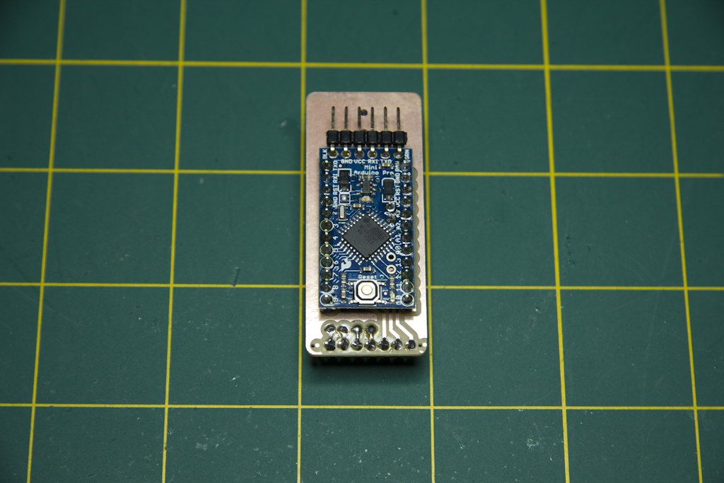
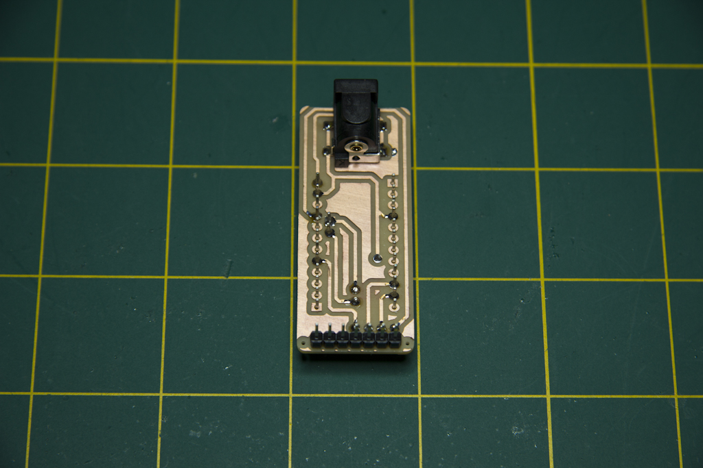
Here, in a few steps are this actual system at work. Right before I started working with the Othermill, I had sent a design out to OSHPark. It’s a dumb little board to allow an Arduino Pro Mini to be connected directly to the back of my MSGEQ7 Audio Visualizer. I thought I’d just mill the board out, since the design adhered to the design constraints already… it’s all 100 mil pins, with a slight tight space between the outside pin array and the two inner analog / I2C pins.
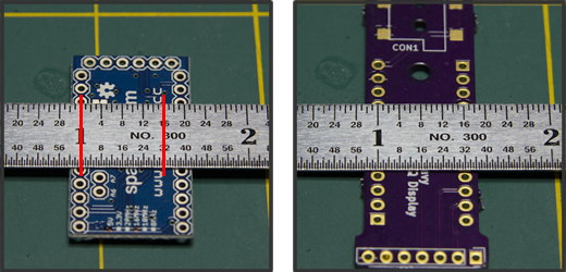
I milled it out in around 45 minutes, and proceeded to solder some vias in place. As soon as I tried to place the Pro Mini, though, I quickly realized I’d screwed up the spacing… it’s 600mil not 500mil. I was too narrow.
One hour later, I’d corrected the problem and produced a fully functional board.
In two hours, I accomplished what would take a board fab four weeks at best to accomplish on my budget. There is certainly an amount of time that needs to be invested in the Othermill to begin producing reliable boards, particularly indexing the board for milling two sided PCBs requires practice, however once those difficulties are worked out, you can go from design to board in such a short period of time, that the learning curve is well worth the investment.
Further, I’m no PCB Milling expert. This is just what I’ve been able to accomplish with common sense and a few tutorials. There are efficiencies to be gained and improvements in quality when I have time to dedicate to the task, and those will get documented as well.
Yep! Board works! Some soldering challenges, but nothing insurmountable. Can only get better. pic.twitter.com/YK4wPRrMiR
— Rheingold Heavy (@rheingoldheavy) February 6, 2016
