June 28, 2014
Spec out the design and figure out what you want the thing to do. Take the vague idea and make it concrete. This step took maybe 10 or 15 minutes, but somehow it was difficult to put the concept I had into words I could work towards. What I came up with was this…
An arduino shield with a variety of SPI and I2C modules that allow a user to practice developing against those communication standards.
Then I thought through several design goals and features, but couldn’t get my brain to settle on specifics. I’ll work on that tomorrow.

June 29, 2014
More spec’ing after you’ve let the concrete set for a day. Decided that I needed to give myself 10 design goals and 10 features that should be worked towards. Design goals would be requirements, functionality would be possibilities.
Design Goals
- Interface with an Arduino Uno R3
- Multiple modules for each communication method to allow working with CS, etc.
- Make it do something useful, so it has long term value.
- Exquisite documentation.
- Use a shift register to bring the very basics to the board.
- Include modules that require both read and write.
- Make it expandable with sockets, headers, terminal blocks, breadboard connections, etc.
- Offer components that allow it to be used as a kit with accompanying documentation.
- Aim for a specific price range, shipped, lower than the cost of starter kits.
- Ensure ease of assembly and testing for production.
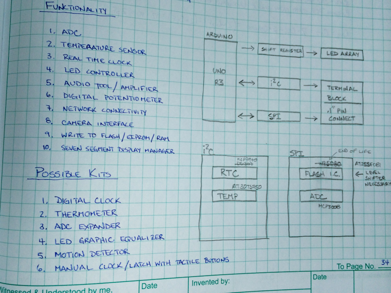
Functionality
- ADC
- Temperature Sensor
- Real Time Clock (RTC)
- LED Controller
- Audio Tool / Controller
- Digital Potentiometer
- Network Connectivity
- Camera Interface
- Write to Flash/EEPROM/RAM
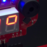
- Seven Segment Display Manager
June 30, 2014
Block diagram… how is the thing going to interact with the system or world around it. Again, the concept is clear in my head, but putting it on paper is still tricky. I think it’s because this is just a new process for me. Putting the idea down in a block diagram though wasn’t as difficult as spending time on digikey finding reasonable parts to select for the systems that match the block diagram: the original flash module I wanted to use was End Of Life at the manufacturer, so I had to switch to another, the RTC I intended to use was just too damn expensive ($3.35!), and the endless reading of datasheets, and more datasheets, and more datasheets.
July 1, 2014
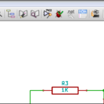
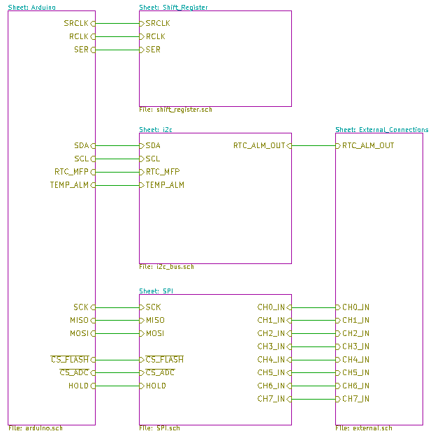
Started work on the initial schematic. Quite a lot of time was spent on how to organize the different modules in ways that make sense… one big schematic? Hierarchical sheets by component? By feature? By protocol? Eventually decided to go with an array of hierarchical sheets with one for the Arduino, one each for I2C and SPI, and one for the output area.
Time on digikey making the final IC part selection. Looooong day of reading datasheets and building matching components to ensure no hiccups with hidden pins. I refuse to use any of the parts in KiCad other than passives anymore, having gotten burned on hidden VCC and GND pins with the Dixie Marseilles project. I’d like to avoid bodging if I can avoid it.
Started building the BOM as I started to develop the list of specific passives that would need to be included to match against the ICs. Need to keep track of things like the RTC Crystal, load capacitors, pull up resistors, thing like that. I’ll add bulk capacitance, headers and stuff like that in at the end.
July 2, 2014
Drawing time! Things are organized and blocked together, now I have to connect things and see if it all makes reasonable sense. Drop in vital passives near the part they belong to: things like pull up / down resistors and bypass caps.
July 3, 2014
Crystal selection and figuring out load caps which means spending time researching theory and selecting sizes. Doing, redoing and re-redoing the math. I’m worried that I’ll have an RTC with some oddly mismatched capacitance in the picofarad range, that will cause it to run slow or fast, or worse, not run at all.
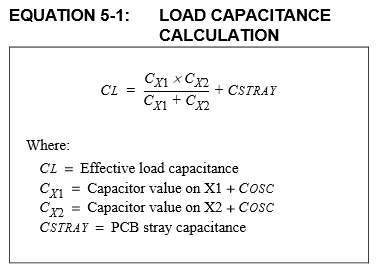
I’m not really confident with this, because the component selection matrix on Digi-Key allows a selection of quite a variety of load capacitances for the crystals, but the datasheet for the RTC specifies that the crystal should have a load capacitance in the 6-9pf range, but it is NOT advised to use 12.5pf crystals. Well, all the crystals on Digi-Key seem to default to 12.5pf when you look at the datasheet. Eventually you just sort of have to commit.
Flesh out the BOM with new required components for the necessary modules: the flash module will need a level shifter, the RTC needs the crystal and matched caps, battery and battery holder and I haven’t even looked at the shift register circuit yet.
July 5, 2014
Cleaning up passives and setting values – decide I’m going with .1uF caps for bypass on the VCC pins of the chips
Cleaning up modules and pins – make sure pin 3 is REALLY what I said Pin 3 is. Back to the datasheets.
Flesh out the BOM with the remaining stuff – passives, headers, etc.
July 6, 2014
Time to start assigning footprints in CvPCB. Start going through the BOM and find footprints for everything. Determine which ones will need custom footprints. Verify EVERY IC FOOTPRINT AGAINST THE DATASHEET!!! This is an unholy and arduous task, particularly since footprints aren’t standardized for reasons best left to the Gods of Electronics to explain. Or rather, there are standards, but some manufacturers don’t care.
July 7, 2014
Building custom footprints for the things that need them. You would think engineers would put the words “THIS DRAWING IS IN METRIC” or “THIS DRAWING IS IN INCHES” in big, bold, clear lettering on their draft documents. But no. Let’s just obfuscate that shit with something like “0.1 (.003)”. Does that mean .1″ with .003 tolerance? Is that .1mm .003″ equivalent? Why must you make this so hard??
July 8, 2014
Final custom footprints and spending time working with the damn tactile button component and footprint. Why can’t I just keep straight in my head how these things work??? First off, it’s a SPST button, that’s momentarily on, so why in the hell does it need four conductive pins?? And why do those four pins have to have pairs that are permanently connected?? AND WHY CAN’T I REMEMBER WHICH PIN IS ALWAYS CONNECTED TO WHICH OTHER PIN??
Start working through ERC bugs. No AGND! Lots of “not connected”. Driving of power pins and grounds … this is typical of KiCAD, and it takes a while to work through what’s really a bug and what isn’t. It helps if you use the “X – NOT CONNECTED” marking in the schematic, but I still don’t understand how to avoid the power pin / gnd errors it always generates.
July 9, 2014
Fix Arduino footprint pinout. I had to add pins for this design, and needed to clean up the silk screen.
Time to import the netlist in PCBNew! Time to have a minor spacing freakout – a lot of the parts are much bigger than I expected.
Edit hotkeys for layer selection, and decide that the interface designer behind KiCAD is a cruel, cruel man. Nothing in this tool seems to work the way every other application does. The entire application can be like trying to add an image to a word document sometimes.
Crystal footprint out of the KiCAD library is wrong, but after drawing my own, the damn thing is so huge anyway, it needs to be replaced. Need to research that later.
The tactile buttons take up way to much real estate too – who knew 6mm x 6mm took up so much room. Go back to Digi-Key and find half sized ones, but after I cut ’em in half, the price just went up by 2x. Great…
Set design rules for trace and via sizes to OSHPark standards.
July 10, 2014
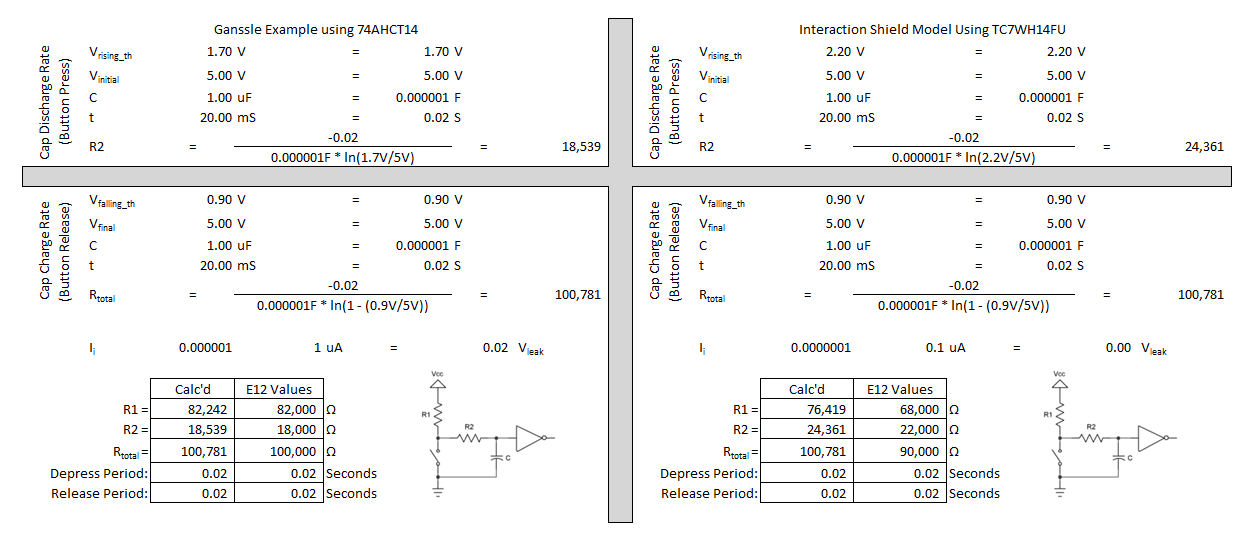
Wow. I went and assembled the shift register circuit on the breadboard and it failed miserably. First off, it needed pull down resistors, but beyond that, it exhibited shitty bouncing with the tactile buttons. After looking at the timing requirements of the datasheet, and the bounce signal on the oscilloscope, it’s pretty obvious that this won’t work at all without incorporating debounce circuitry. Off to learn about switch debouncing from Jack Ganslle – did the math. Re-did the math. Decided it would be best to follow along with the datasheets Ganslle talks about so that I can do an apples to apples comparison.
This is what my buttons look like on the scope…
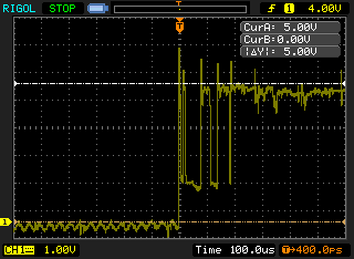
Not feeling too confident in the numbers I came up with.
July 11, 2014
Layout and routing. Layout and routing. Had to take a step away from the computer to let brain decompress, watched Totoro, came back and had the insight that the tactile switches only need +5V from the power plane, I didn’t need to run signal paths from what will be SCLK, SRCLK and SER, so no need to route all that shit everywhere.
My brain can get very full sometimes, and sometimes the best solution is no solution. As the Lord Humungous once said, just walk away.

July 12, 2014
More debounce calculations. Numbers not adding up. Should be 20 mS but the formulas don’t make any sense. Decided to change from the TI six input inverter to a smaller one to save on footprint size and the new numbers from the datasheet didn’t work. Reworked and reworked and realized I was using Rtotal instead of R2 for the discharge rate and wasn’t subtracting 1 from the RC time constant for the charge rate.
Level shifter is too damn big. I mean that thing takes up a monstrous amount of space on the board. Have to find a different solution… two bit shifter + voltage divider? The WP pin just needs 3V3, but doesn’t change state rapidly (I hope), so I can break that out to a jumper, but HOLD? I don’t know. Since I don’t know, play it safe and make sure it passes through the level shifter and not some hokey voltage divider bullshit, Dan.
* * *
Late push to get everything done as a first draft. First trip through DRC showed only the pads of the Schmitt Trigger being too close – which needs to be checked – and nine disconnected pads due to the funkiness of laying out a two sided board… hard to keep those copper pours from getting sliced and diced to pieces.
To do:
- Pretty up the reference silk screen. Common sizes for all fonts on all components. Large = .7 / .15 Small = .5 / .1
- Add required explanatory elements to the silk screen such as “CLOCK, DATA, LATCH” button, descriptions of jumper purpose and position, etc.
- Add Rheingold Heavy “R-Bar” solder mask relief.
- Add contact info, project name, rev #, etc to silk screen.
- Verify all pins on all components… verify all Vcc and GND pins are connected for all devices.
- Verify footprint size for all components.
- Double check the footprint for that damn schmitt trigger.
July 14, 2014
Well that was dumb! I re-annotated the schematic and now my layout is entirely disconnected. It didn’t simply relabel the passives, it maintained their location on the layout and then renamed them, meaning everything has to be rerouted! It will be cleaner in the end but dammit! Time to dive into it…
* * *
Finished cleaning everything up and added the explanatory items to the silk screen. Started doing the footprint check and WHAM!, when cleaning up the footprint for the level shifters, the schematic allowed the layout to show DIR connected to a bypass cap but not Vcc for the level shifters. Kind of a big deal. That would mean the pin that determines which direction the signal is being translated, 5V to 3V3 or vice-versa, would be floating. Oops.
July 15, 2014
To Do:
- Clean up Arduino footprint of non-essential silkscreens
- Generate Gerbers
- Verify drills, pads and silkscreen in gerbview
Missing references for the two level shifters. At some point they were made invisible.
Wow… all the front-side copper components were connecting directly to the power plane, and their decoupling caps were just sitting there. Had to add keepout areas around all the Vcc pads to allow traces to run cleanly to the respective decoupling cap and prevent the copper pour from touching the pin directly.
Generated the gerbers and pulled them up in Gerbview. Cleaned up a few things like rotating references on some of the backside passives, and removing the “ARD1” label, but nothing major. Still and all, I always feel nervous about sending the gerbers to OSHPark… like someone is going to get the files and go, “YOU HAVE NO BUSINESS DOING THIS! IT CAN’T POSSIBLY WORK!”.
Boards ordered.
[masterslider id=7]Spent time in excel putting the finishing touches on the BOM and cross checking the Digi-Key part numbers. Parts order placed.
July 16, 2014
OSHPark has assigned the design to a panel and sent it to the fab. Expected shipping before the end of the month!
July 24, 2014
Great. According to UPS, the parts from Digi-Key were delivered, but I never saw them. The package tracking says, “Left at front door 4:03PM” but I was in and out of my apartment that afternoon and no one ever knocked, and no package was ever there. Called Digi-Key and had them open a package trace, but they say it will take until next week to hear back from UPS.
OSHPark has depanelized the boards and they’re being shipped.
July 29, 2014
Boards arrived! They always seem smaller in person after having stared at PCBNew for hours and hours.
Digi-key has sent another parts shipment while we wait to hear back from UPS.
I got stung by a jellyfish relative called a “White Feather Hydroid” on the back of my right hand and between the fingers. It’s making it nearly impossible to type. I’m going to have to stay away from the computer for a few days.