So you’ve just created a stunning design, a feat of engineering that would make you millions through crowdsourcing if only the masses could see your project through the phalanx of cash filled dumptrucks VCs are driving to your house daily. This is when you realize: there is no way in hell you can solder all of that by hand! Time to start talking to contract assembly houses.
More realistically, you’ve just come up with a design that you want to share with your friends, or take to an art exhibition, or you’ve sold 100 boards through Tindie and now you need to get them assembled by a facility that has a pick-and-place machine ready to go. Hopefully this will give you guidance on how to prepare for that, and introduce you to some of the nomenclature that you’ll start to run into when you step out of design and move into fabrication.
I use KiCad (the version I’m using is v2013-07-07 BZR 4022-Stable) as my EDA tool of choice, because the price is right, and I’ll be using it exclusively in this post to step you through a full design for assembly. To make this semi-realistic, I’m going to throw together a little 555 circuit, so we can have a mix of through hole and surface mount pads, that will result in having to do some customization to get good gerbers on the back end. The circuit is a basic 555 astable multivibrator that blinks an LED at a variable rate governed by a potentiometer. I’m also going to focus on the specifications you would need to follow in order to contract with Small Batch Assembly to do your work. Other design houses I’ve been in contact with have different specs, but once you understand how to design for Small Batch Assembly, you’ll be able to modify the workflow to provide files to the others.
Design For Assembly Starts Before You Start
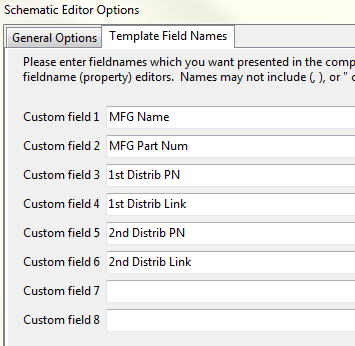
Before you lay a single component down on your schematic, it will be very helpful for you to do a quick customization inside KiCad first. We need to add six custom fields to our component properties that will provide a lot of detail in the Bill of Materials (BOM) later. MFG Name and Part Num are the name of the component manufacturer (Texas Instruments, Yageo, etc), and the part number from the manufacturer. The Distrib PN and Link are the distributors unique part number and a link back to the product at the distributor’s site. If you’re going the route of an assembly house, chances are you’re ensuring second sources for your components, so you want to capture that data here as well, hence the 1st and 2nd Distrib fields. To add these, launch EESchema, click on Preferences in the menu, select Options and then go to the Template Field Names tab.
- MFG Name
- MFG Part Num
- 1st Distrib PN
- 1st Distrib Link
- 2nd Distrib PN
- 2nd Distrib Link
With that done, you can start building your schematic. You’ve just added some pretty serious complexity though, since you need to track all of that data for each and every piece on your board. This is, in fact, just as tedious as it sounds. It’s helped a little bit by the use of copy and paste with a component, as that will copy the metadata for it as well, but a 100Ω resistor will be entirely different metadata from a 1000Ω resistor, so, you can see how bad this can get fast. In KiCad though, there’s no real way around it*, so just be patient with it and realize you’re getting what you paid for. The details you need can generally be copied straight off the part matrixes that you get at Digi-key or Farnell / Element 14, or Mouser, so it’s easy to get into a quick rhythm. Make sure you’re capturing a link to the datasheet as well as all the information up there.
There is a section in the component properties for describing the footprint, but don’t worry about that right now, we’ll fill that in with the CvPCB tool. However, while you’re in the properties for each component, uncheck the “Show Footprint” selection, because that will only clutter everything up later.
Fiddling Fiducials
[masterslider id=18]Pick-and-place machines need some visual reference for their robotic eye to use as a guide for where they are on the board. Those visual references are called “fiducials“, or simply fids. We’re going to need to add some of these to our schematic so that they’ll be picked up in the BOM, by CvPCB and imported into the PCB as well. As far as the schematic is concerned, it’s really just a graphic – no pins associated with it, so don’t add any in the Component Editor. In fact, when we bring them into the PCB Layout, we want these things isolated from everything else around it, no traces / no copper pours. Just make sure the component name is “Fiducial” and that the reference designator is “FID”, so when the schematic is annotated you get, “FID1”, “FID2”, etc. We want three of them on our schematic, but it’s ok to just stick them over to the side.
Continue on with your design, filling in the detailed aspects of each component as you go. Follow whatever workflow you have established, including testing ERC, annotation and generating netlists. None of that will be affected by the increased metadata you are capturing.
Put Your Footprint Down
Once you’ve finished your annotation and generated your netlists, it’s time to go into CvPCB (I have no idea what that stands for) and associate footprints with your components. Chances are, you’re going to need to create a custom footprint or two (at the very least for the fids), so we’ll need to think through how we create the footprint to make sure it gets placed correctly at the assembler.
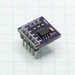
First, figure out what sort of feeding mechanism you’re going to need to accommodate for. In the case of our 555 timer, it’s going to be a reel of parts on tape, although other ICs can be supplied in tubes. Small Batch Assembly can handle most of that, provided you meet their specs. According to the datasheet, we have an 8 pin Small Outpine package (8SO). However, the datasheet doesn’t contain any reel information. It does say, “The package drawing(s) in this data sheet may not reflect the most current specifications. For the latest package outline information go to www.maxim-ic.com/packages”, though, so a quick trip over to the Maxim homepage pulls up a link directly showing all the reel data you could want.
Turns out, our part is going to be fed to the pick-and-place with the sprockets on the top and Pin 1 in Quadrant 1. This is how we want to create the part in the module editor – using that orientation. Because of this, when we start doing layout and start rotating it left and right to figure out how to place it, we’re rotating from a standardized 0° orientation. This can be potentially different for each part. There is no “Pin 1” really for the battery holder, so you absolutely have to look it up to see how it’s oriented on the reel.
[masterslider id=19]Secondly, you have to think through whether you want solder to exist on the pads you’re creating for your custom parts. For example, with the 555 IC, we need to have solder stenciled onto each of the copper pads for our chip. However, for the battery holder, it’s designed so that the negative pole of the battery just presses directly to bare copper on the PCB – no solder should be put there. The way we take care of this is to check the list of “technical layers” associated with each pad, in the Pad Properties, for our component. If the pad should receive solder, then F.Paste should be checked. If the pad should remain clear, F.Paste should be unchecked. A checked box means the pad will be exposed through the solder paste stencil, and consequently squeegeed with solder goo during assembly. KiCad is smart enough that all PTH connections should have the F.Paste check mark cleared by default as well. If you have some strangely intricate part that is a mix of many of these, you’ll be able to better catch mistakes when we double check our gerbers later. I find going through screen after screen of metadata very tiring on my eyes and I can get lost in the details very quickly.
Small Batch Assembly suggests allowing the ground pad of the battery holder to remain exposed through the solder paste stencil, that way a small amount of solder will build up on it and allow a far more reliable mechanical connection with the battery. For production boards this is excellent advice. I am only leaving it bare here because I wanted to demonstrate a part having different paste layer properties applied to it’s pads. They also wanted to caution against putting any unmasked vias in the area where the negative body of the battery will be in physical contact with the board, to prevent short circuits.
Thirdly, when creating the footprints for your fids, this is a good spec to follow: round, surface mount pad, .020″. Under “Local Clearance and Settings” in the pad properties, set a Net Pad Clearance and Solder Mask Clearance of .040″ each. This will ensure that both the copper layer and the solder mask are kept far away from the visualization dot. Also just double check the technical layers are correctly specified: F.Mask layer checked / F.Paste layer unchecked.
Finally, I hate to say it, but you cannot rely on the supplied footprints in the KiCad libraries to be correctly oriented. They are generic footprints and packaging may differ from one manufacturer to another. Our 555 component is a prime example. The packaging drawing on Maxim’s website shows Pin 1 in Quadrant 1, but the S08E footprint within KiCad has Pin 1 in Quadrant 3. When the pick-and-place arm went to place the piece, it would be rotated 90° off. The important thing to have here is consistency. It’s very easy to go through and use a spreadsheet application to modify EVERY rotation spec, but one or two errors here and there would prove very difficult to deal with.
As an aside, this might be the most brilliant thing any engineer, draftsman or technical writer can ever put on any document, short of “Don’t Panic” in large friendly letters…
Once you’ve finished creating all the necessary footprints, you can finish up in CvPCB by assigning the footprints where they go. After you’re done, go back into EESchema and click on Edit then Import Footprint Selection to pull all the associations back into your component metadata fields. When it asks “Do you want to force all the footprint fields visibility” I always select No, but if you select Yes, then prepare for a TON of cruft to be blasted into your schematic. If you have four or five components it’s not bad at all, but even with the small amount we have in here, it can really make it cluttered.
[masterslider id=20]Layout and Routing Considerations
Provided you created all your parts correctly in the module editor you should be able to twist and twiddle your parts all over your board to your hearts content, and each rotation will dutifully be recorded for you by KiCad in the background.
When you get to placing your fiducials, you want to place them in the corners of your board, as far apart from each other as possible. Ideally, you want to have a “master” fid, FID1, and then the other two sharing only the X or the Y axis with the master. I place FID1 in the bottom left corner, FID2 upper left and FID3 bottom right. FID 1 and 2 share a common Y-axis value, and FID 1 and 3 share a common X-axis value. Because we set the Net Pad and Solder Mask clearance properties, you should see no copper pour near your fids when you “Fill or Refill”. Also, it should prevent you from routing traces in that area as well.
Once you have your fids placed correctly, grab the “Origin Point” tool and click in the dead center of FID1. This isn’t strictly necessary, as all locations are relative to each other, but when I pull up the placement file later, I find it easier to see points in relation to the fiducial – meaning the distances in this case should be 1.5″ or less, rather than the distances you’ll get based on KiCad’s arbitrary origin point which is located somewhere outside the orbit of Neptune.
From Small Batch Assembly: That is a good party-line. The reality is I can deal with boards with no fiducials, but I wouldn’t want to have to build even 25 of them as it requires a manual step per-board. Final guidance is that I just need two fids in opposite corners of the board. The bare copper dot can be as small as .5mm w/ a 1mm guard area.
Generating and Proofing Gerbers
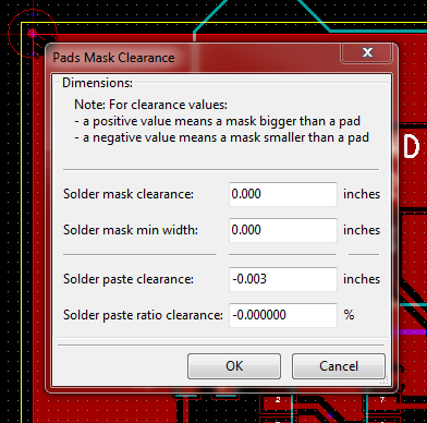
After you’re done with all the layout and routing, it’s time to spit out some gerbers, but before we do that, another global customization needs to be applied, this time in PCBNew. By default, the size of the solder paste stencil cutout will be the same as the solder mask cutout, which is bad. You want just a hairs-width smaller size on your stencil cutout over the pad to allow for little mis-alignments along the way and to ensure that you get solder paste only on copper pad. There is an extensive document published by the IPC that covers the topic of Solder Paste Stencils in minute detail, and for the mere cost of $41 you can purchase a non-printable copy of it for your review. Let me boil it all down for you: just launch PCBNew, select Dimensions from the menu and Pads Mask Clearance – set your solder paste clearance to -.003″. I grabbed that value from the Texas Instruments footnotes that appear in every datasheet they have for surface mount packaging components. For example, check out page 20 of the 74HC595 Datasheet. The truth is that this spec might be different from chip to chip, particularly as you get down into the small pitch parts like TSSOP. If you’re to the point of sending your boards to assembly houses for manufacture, I suspect you’ve been reviewing datasheets and footprint documentation all along the way. Along with pin pitch and package width, now you just have to remember to look for solder paste stencil details as well and incorporate that into your design by modifying the clearances for the pads in the Module Editor.
After setting our solder paste clearance, we’re ready to generate Gerbers. Click File then Plot and make sure all the appropriate layers are selected. I believe the Paste layers are unchecked by default so verify those. You also want to check “Use auxiliary axis as origin” before clicking “Plot”.
Now that we have the gerbers, we need to proof them, and for that we could use GerbView, which comes with KiCad, but do yourself a favor and download Gerbv instead. When you’ve pulled the gerbers into your viewer of choice, have a look around and check for this sort of stuff…
- Anything that’s supposed to be a copper pad, is a copper pad.
- Anything that’s a copper pad, is exposed through the solder mask.
- Anything that’s a copper pad and is supposed to receive solder, is exposed in the Paste layer.
- Anything that’s NOT supposed to receive solder is NOT exposed in the Paste layer.
- Anything that should appear on the paste stencil is smaller than the solder mask relief that surrounds it.
- The other stuff you look for in gerbers, like bad silk screen placement, unnecessary text, bad copper pours, etc
When I generated the gerbers for this, it turns out I originally had forgotten to disable the paste layer for the GND pad of the battery holder. Consequently, it was there in the gerbers. It was fairly easy to just right click on the pad in PCBNew, select “Edit Pad” and uncheck F.Paste as a technical layer.
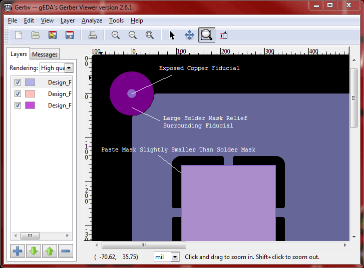
[masterslider id=21]You should also check that the fiducials are clear and clean – they should appear as a single dot of copper floating in a sea of exposed FR4.
Your Design is the BOM
We have very pretty gerbers now but this is useless if we can’t tell the pick-n-place machine where to put it and how to rotate it for a successful placement. We do this by providing Small Batch Assembly with the BOM for our design. Unfortunately it’s not as simple as one click and done, we have to export the BOM, export the placement file, combine them, and then edit them to match the headers required by SBA. However, because we spent all that time earlier loading all metadata into our schematic, all we really have to do now is a little cutting and pasting.
To generate the BOM, go back into EESchema and click on the BOM button (up by the netlist and CvPCB buttons). Select your Output format as “List for spreadsheet import (by ref)” so that we group everything by reference designator, ie: R1, R2, R3, C1, C2, etc. Select the comma as your Field separator so we create a CSV file and add to the list your Component Location, footprint and datasheet fields and check “All existing user fields.” Click OK to generate the BOM, and note where it saved the file (should be in the same location as the rest of the project files).
Now create the placement file by going back to PCBNew clicking on File then Fabrication Outputs and selecting Modules Positions (.pos) File. With Units: inches and Files: One file per side all that’s really left is the Footprints selection, which I don’t really understand. In the module properties page, there is a setting called “Attributes”, with the settings of Normal, Normal+Insert and Virtual. If your module is set to Normal or Virtual, then it will not appear in the placement .pos file. If it’s set to Normal+Insert it will be included. Apparently, the “insert” only means “put it in the placement file” (check the KiCad manual, section 12.11 I think).
With the BOM and the Placement file created, you need to combine them so that you have a single CSV file that matches the headers specified on the SBA Column Name And Extended File Definitions spec.
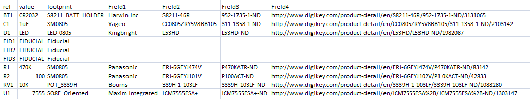
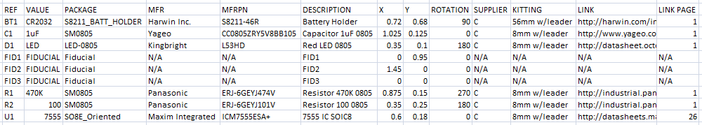
Here is a sample of the raw BOM output…
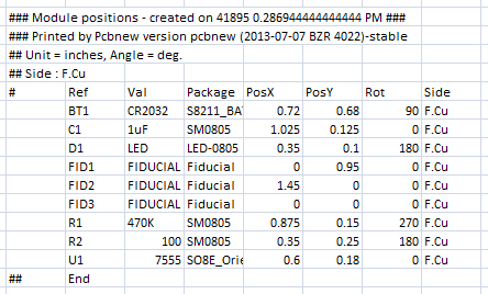
Here is a sample of the raw .POS output…
Here is it all swizzled together, using corrected headers…
I’ve included the final few headers as required by the Small Batch Assembly specifications and the information on those can be found through the link above.
Using these two files, you would be able to use the instant quote system at Small Batch Assembly and have them solder your components for you!
I’d like to thank Bob Coggeshall of Small Batch Assembly for the time he took to read through this documentation and provide his feedback!
Click here for the files associated with this post at the Rheingold Heavy GitHub repo.
Part 2 will focus on PCB panelization…