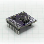
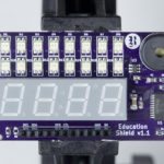
Over the past two weeks, I’ve had a string of prototype failures that are entirely attributable to one origin: me. Generally, I (like to think I) have exceptional attention to detail which delivered quite a few proofs of concept that all worked the first time. This invited some workflow complacency on my part which resulted in those mistakes. Unlike software bugs, a bug in your hardware design costs real money, this time in the form of over $400 worth of quick-turn board orders.
The Problems
Across two prototypes I’ve made the following mistakes…
Drills
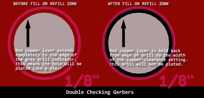
Mounting holes, called “non-plated through hole” or NPTH drills, whose very name suggests that they shouldn’t be plated, were in fact plated. There was no copper relief on either side of the board, so 5V and GND shorted out the entire board directly.
Clearances
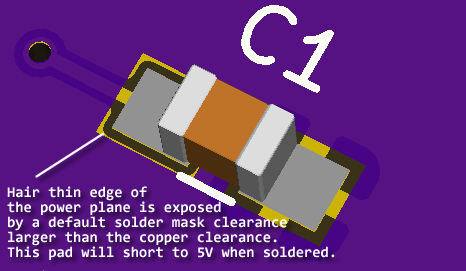
The solder mask clearance, which I had set in BZR4022 version of KiCad to 0.000 (lazy but effective), was reset when I upgraded to RC1 to 7.8mil. The problem comes about because the copper clearance was set to 6mil. All the components were topside, so the solder mask relief exposed not just the pad, but a hair thin edge of the 5V plane surrounding the pad as well. As soon as any solder was applied, every single pad on the board shorted to 5V directly.
Pin Out Screwup 01
VDD and VSS pins were swapped on the primary driver IC for one of the boards.
Pin Out Screwup 02
While I very carefully verified the size of the footprints on one of the boards, it didn’t occur to me to match up the pin out for a pair of SOT23 magnetic sensors… so I never noticed that what I wound up with had the ICs ground pin connected to the micro’s pin, and the sensor output connected to the ground plane, frying the chip instantly on power up.
Pin Out Screwup 03
When I created a QFN footprint, I was very deliberate in setting the pad size and spacing. But somehow I laid the pins out as a mirror image. I cannot fathom how I did that.
Parts Ordering
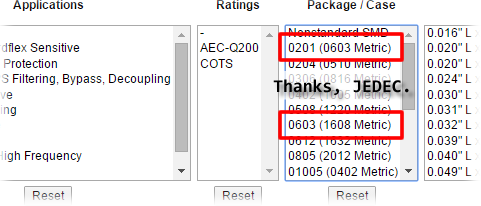
I ordered a bunch of 0201 size bypass caps, intending to buy 0603. Why? Because when I looked for the part on Digi-Key they say “0201 (0603 Metric)” and my brain saw that last part and just ran with it.
Disconnected ComponentsThe user accessible header on the right was left entirely disconnected; no traces were run to it.
Modifying Design After Sending Out For Fab
I got distracted and started replacing one style of LED with another that had a different footprint, saving all the time, while forgetting that I had a prototype coming with the older footprint and still needed to get a paste mask stencil made.
Root Causes
When I look over that list, I immediately see that a little diligence on my part would have prevented nearly all the failures. If it’s checking the BOM against the footprints before ordering, or double checking the gerbers, little niggling checks off the check list would keep a lid on this sort of thing.
Let’s do some root cause analysis…
Plated Mechanicals: this occurred because I didn’t recalculate the copper pours before generating gerbers. Further, if I had double checked the gerbers before submitting them for fabrication, I would have noticed that there wasn’t relief around the drills on either side of the board immediately.
Solder Mask Clearance: when you set something and don’t have to touch it for two or three years, you will forget it’s there… and then when it’s suddenly no longer a default it will catch you out. However, a double check of the gerbers would have shown that little rim of power plane around the pads. I might not have seen it though.
Swapped Pins: this is just sloppy. No excuse. I probably put those footprints together later in the day than usual which means I wasn’t quite as focused, but I must have used the wrong datasheet to assemble the pin out for that QFN.
0603 is 0201: giving myself a pass on this one because it’s not the first time or the last time I’m going to switch out numbers accidentally. It’s a mistake, but an honest one. A double check of the BOM against the footprints would be wise though.
Disconnected parts: hey, Dan. You do realize that there’s a utility built into KiCad that checks for this automatically, right? Did… did ya not think to check it?
Changing a design during fabrication: this is the essence of this whole post, and a great segue…
Electronics Design Workflow
The core of having an electronics design workflow is creating a standardized method by which you bring a project from point A to point W, defining what happens at points B-V along the way. Having spent a lot of time working as a scuba instructor, we drill this sort of thing into students heads with (admittedly awful) acronyms like BWRAF. For prototyping and manufacturing, I think a checklist would serve nicely: nothing goes out for fabrication or assembly unless there’s a check in each of these boxes…
Before Layout
- Double check your design rules against your fabricator of choice, and ensure clearances are correct.
- Set up your project correctly by specifying all the necessary clearances: minimum trace width, minimum copper clearance, via drill vs. size, solder mask clearance.
Before Generating Fabrication Gerbers
- Recalculate your copper pours.
- Run the Design Rules Check utility.
- List unconnected pads.
- Verify each manufacturers part number against their respective footprints.
- Verify each schematic IC pinout vs. the footprint pinout vs. the datasheet.
Visually Inspect Gerbers
- Drills are correctly placed.
- Copper relief around mechanicals.
- Correct pads are exposed through paste layer.
- Silkscreen references are clean.
- Comments to the fabricator are present in a comments gerber file.
Before Production Runs
- Check that no components overhanging the board edge conflict with others on the panel
- Check the footprints against the parts order at least three times
- Verify order quantities
- Verify component packaging (tube vs. reel vs. bulk, etc)
- Verify kitting method and prepare tags / stickers as necessary
Finally, when a design is out for fabrication or assembly, don’t modify the design without preserving a copy of all the design files for the version being created. When it comes time to test, and you went and rerouted all the traces, you’ll drive yourself crazy trying to find a via to use as a test point, or figure out if a chip was soldered on backwards.
Electronics Design Workflow Bottom Line
It’s easy to be methodical when doing the engineering work of putting a design together. Calculating the value of I2C pull up resistors, or designing an oscillator subsystem are the things that we really get into (and most others look at us as being nutty for enjoying). Being calculating in your process should extend beyond the design of your product, right into establishing that process in the first place.
That’s when you stop being a hobbyist, and start being professional.
For more KiCad tutorials, Click Here.
