We can pull back all the information we want from the chip, so let’s work on sending some data for it to store instead by focusing on programming the AT25SF081 memory.
Objectives
- Determine which opcode is used to program the array.
- Understand how the array handles writing past the end of a page boundary.
Background
AT25SF081 Tutorial 02: Reading Memory Byte
SPI Signals
Adesto AT25SF081 Datasheet
Schematic
Education Shield – AT25SF081 Flash Memory Subsystem
Setup
For this module, you’ll need the following equipment:
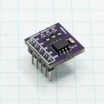
- I2C and SPI Education Shield or the AT25SF081 Flash Memory Breakout Board
- Arduino UNO R3
1. Mate the Education Shield with your Arduino UNO R3. If you’re using the AT25SF081 Flash Memory Breakout Board, connect 5V to 5V, 3V3 to 3.3V, GND to GND, HOLD to Digital09,CS to Digital10, MOSI to Digital11, MISO to Digital12, and CLK to Digital13. That’s a lot of pins!
2. Connect your Arduino to your USB cable, and use the Arduino IDE to upload the “Bare Minimum” sketch from the Basics section of the Examples.
Working with the HOLD pin is not necessary for any of the tutorials, it is only included on the breakout board for completeness. In the sketch it will always be set as an output in a high state, and on the I2C and SPI Education Shield, the pin is tied directly to the 3V3 rail on the PCB.
Programming the AT25SF081 Memory Array
You can write anywhere from a single byte of data up to 256 bytes in a single shot to the AT25SF081. To do this, you use the opcode 0x02. The process you follow is a little more involved than the method used for reading from the array…
- Set the WEL bit.
- Send the program opcode.
- Send the starting memory address you want to write to.
- Send the data you want to program to the memory array.
Both setting the WEL bit, and the program command operations need to be wrapped inside bringing the chip select pin low then high.
Memory Pages
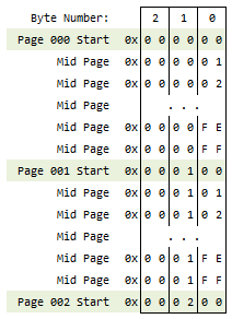
It is important to understand how the memory is organized inside the chip and how that will affect your write commands. Each byte inside the chip is part of a discrete page of memory, laid out in chunks of 256 bytes. You know if you’re at the beginning of a page because the least significant byte of the address will be a zero.
Single Byte Program
If all you do is write a single byte to the array at a time, then everything will function just as you expect. You specify the byte address, write a single byte and move on from there.
Multiple Byte Program
Writing more than a single byte can have an unexpected consequence. Multiple bytes of data sent with a single command are at risk for overflowing the end of the page. If that happens, the chip will automatically begin writing the subsequent data to the start of the same page, which is a little weird. This is very important because if you begin overwriting previously programmed data, you will just store gibberish. Overwriting flash memory is not supported. If you want to write new data to a byte, it has to be erased first due to error correction code performed within the chip itself. Care must therefore be taken to make sure you know where your writing your data, how much data you’re writing, and how much free space within the page you have to work with.
Programming a Single Byte of AT25SF081 Memory
We’ll start off by storing a single byte of data in our array. Program and Erase commands are responsible for chewing into the endurance of the chip, so our test code will be carefully designed to only run once if at all possible. We can use the previously completed sketch as a starting point, since we’ll want to confirm our activity by displaying before and after output.
We don’t have to change the existing code so much as we need to make some additions to it. The only real change is to move the chip initialization into it’s own function, just as we did for the I2C devices. For additions, firstly we need to add the Program Byte opcode 0x02 and the Write Enable opcode 0x06 to our declarations section (and an opcode for reading the status register, but we’ll get to that). Since this is just an example, we’ll also hard code the data that we’re going to program to the memory as well. The major change will be in creating a function that performs all the steps listed above to perform the program routine. I’m going to call this function writeByte.
Set the WEL Bit
The Write Enable bit is a part of Status Register 01, and it is set and cleared using the Write Enable opcode 0x06 and the Write Disable opcode 0x04 respectively. For the most part, we only need to set the WEL bit, because it will automatically be cleared after the successful execution of a program command.
|
1 2 3 |
digitalWrite (CS_AT25SF081, LOW); SPI.transfer (OPCODE_WRITEENABLE); digitalWrite (CS_AT25SF081, HIGH); |
Program the Array
The WEL bit is now set so we can perform a program operation. First the opcode is sent, then as we did when reading the array, we have to break the starting 24 bit address into discrete 8 bit chunks, and we’ll use the same commands to accomplish that. Once the address is clocked in, you can start to transfer the data over MOSI to the chip.
|
1 2 3 4 5 6 7 |
digitalWrite (CS_AT25SF081, LOW); SPI.transfer (OPCODE_PROGRAM); SPI.transfer ((writeAddress & 0xFF0000) >> 16); // Byte address - MSB Sig Byte SPI.transfer ((writeAddress & 0x00FF00) >> 8); // Byte address - MID Sig Byte SPI.transfer ((writeAddress & 0x0000FF) >> 0); // Byte address - LSB Sig Byte SPI.transfer (dataToProgram); // Write data to address digitalWrite (CS_AT25SF081, HIGH); |
You can immediately see that for both setting the WEL bit and the program commands, each is surrounded by code to manipulate the state of the chip select pin. The WEL bit change doesn’t take effect until the pin is brought high to latch the value in, so it has to be separated from the rest of the commands. If you tried to do it all at once, the program commands would be ignored by the AT25S081 because the WEL bit would still be cleared.
The full function then looks like this…
|
1 2 3 4 5 6 7 8 9 10 11 12 13 14 15 16 17 18 |
void write_byte(long writeAddress, byte dataToProgram) { // Set the WEL bit digitalWrite (CS_AT25SF081, LOW); SPI.transfer (OPCODE_WRITEENABLE); digitalWrite (CS_AT25SF081, HIGH); // Write a byte of data to writeAddress digitalWrite (CS_AT25SF081, LOW); SPI.transfer (OPCODE_PROGRAM); SPI.transfer ((writeAddress & 0xFF0000) >> 16); // Byte address - MSB Sig Byte SPI.transfer ((writeAddress & 0x00FF00) >> 8); // Byte address - MID Sig Byte SPI.transfer ((writeAddress & 0x0000FF) >> 0); // Byte address - LSB Sig Byte SPI.transfer (dataToProgram); // Write data to address digitalWrite (CS_AT25SF081, HIGH); } |
Testing and Timing
Read commands are executed instantaneously, since all you are doing is sampling the existing state of a NAND gate array within the chip. Program and Erase commands change the state of those gates and that takes a bit of time, so you need to accommodate that delay after any program / erase cycle.
The method for doing this is polling the READY/BUSY bit, bit 0, in Status Register 01. If the chip is executing an erase or program command the bit is set automatically, and all you have to do is keep checking to see when the bit gets cleared. The datasheet defines the lengths of time it takes to write or erase sections of the memory array, but also says it’s more efficient to simply check the state of that bit, rather than doing a hard coded time out based on the times listed. Fair enough.
It’s very simple to poll the busy status of the chip, and we’ll create a function called checkStatus to do this…
|
1 2 3 4 5 6 7 8 9 10 11 12 13 14 15 |
void checkStatus() { byte readyBusy = 1; // Preset the readyBusy variable as BUSY byte JUNK = 0xFF; // Junk data for MOSI output digitalWrite (CS_AT25SF081, LOW); SPI.transfer (OPCODE_READSTATUSREGISTER01); while (readyBusy == 1) { readyBusy = SPI.transfer(JUNK) & 0x01; } digitalWrite (CS_AT25SF081, HIGH); } |
We create a small variable called readyBusy and set it equal to 1. Chip select is brought load and we clock in the Status Register 01 Read opcode. Then we repeatedly load readyBusy with the value of the least significant bit of Status Register 01, the RDY/BSY bit, and wait for it to evaluate as cleared. Therefore, as long as the chip is busy, it will stick in this while loop, which is a quick and dirty way of pausing our sketch while the chip is performing some task. The datasheet says that after you clock in the read opcode, subsequent clocks cause the value of Status Register 01 to be transmitted over and over and over again, so you don’t have to constantly cycle chip select and resend the opcode.
Mind you, this is definitely quick and dirty. It’s blocking code, which means that your Arduino is prevented from performing any other task while this is executing. It’s also somewhat indeterminate as to what happens if there’s a problem with the SPI bus during this time. What happens it if jams up and just sends back 1s indefinitely? The code will hang at this point and never evaluate to 0, ending the loop. More robust code would want to evaluate against a timer of some sort and if the maximum length of time has passed that should have been necessary to execute the command, break out of the while loop and blink LEDs or something to indicate an error has occurred.
But for our purposes of testing the functionality of the chip, this is good enough.
Quick Check of Execution Logic
Think through the execution of the program and what we want to have happen. Ideally, we want to see a whole bunch of FF values indicating that everything is in an erased state, then after we program our byte, we would expect to see one of those values changed to whatever value we’re sending (my code is sending 0xCC). Critically, we want to verify that it changed because of our code by showing the value of the byte before the program command and then the value of the byte after the program command.
If we just upload this sketch with the execution of the program opcode in Setup as we’ve done in the previous two sketches, we screw things up because it will execute immediately after upload, then execute again when you open the serial monitor. As a result, you won’t see any change occur because it already happened right after you clicked upload.
That means using our buttons will come in handy. We’ll tie the execution of our little memory program test to the Latch button so we can cause it to fire off when we choose… meaning after we upload and get the serial monitor window open.
Here is the full sketch including all the changes.
|
1 2 3 4 5 6 7 8 9 10 11 12 13 14 15 16 17 18 19 20 21 22 23 24 25 26 27 28 29 30 31 32 33 34 35 36 37 38 39 40 41 42 43 44 45 46 47 48 49 50 51 52 53 54 55 56 57 58 59 60 61 62 63 64 65 66 67 68 69 70 71 72 73 74 75 76 77 78 79 80 |
/* A sketch to program data to the 8-Mbit AT25SF081 Flash Memory IC. This sketch will write a single byte of memory to the memory address specified in the some24bitLocation variable within Setup. The code supposes the use of the Education Shield, but if you're using a breakout board, connect the CS pin to Digital 10, HOLD to Digital 9, and the SPI pins in their usual locations. Website: https://rheingoldheavy.com/at25sf081-tutorial-04-programming-memory Datasheet: http://www.adestotech.com/wp-content/uploads/DS-AT25SF081_045.pdf */ #include // Include the SPI library SPISettings AT25SF081(8000000, MSBFIRST, SPI_MODE0); // Sets the pin values for the AT25SF081 and MCP3008 const int CS_AT25SF081 = 10; // Flash Memory Chip Select - Active Low const int holdPin = 9; // HOLD Pin - Active Low // Set bits for the various Flash IC OpCodes (see datasheet) const byte OPCODE_SLOWREAD_ARRAY = 0x03; // Memory read up <= 50Mhz (see datasheet) const byte OPCODE_FASTREAD_ARRAY = 0x0B; // Memory read up <= 85Mhz (see datasheet) const byte OPCODE_WRITEENABLE = 0x06; // Enable programming const byte OPCODE_PROGRAM = 0x02; // Write command const byte OPCODE_READSTATUSREGISTER01 = 0x05; // Read Status Register 01 const int programButton = 7; // LATCH button used to set resolution void setup() { Serial.begin (9600); pinMode (programButton, INPUT); AT25SF081_init (); Serial.println ("Press the LATCH button to execute the PROGRAM command..."); Serial.println (); } void loop() { int buttonPressProg = 1; // Determins if this is the first button press long some24bitLocation = 0x000000; // Starting address we'll use to R/W byte someData = 0xCC; // Some data to write to memory byte pageData[256]; // Array of bytes to hold a page of data while (digitalRead(programButton) == HIGH) { if (buttonPressProg == 1) { buttonPressProg = 0; SPI.beginTransaction (AT25SF081); Serial.println ("BEFORE..."); readPage (some24bitLocation, pageData); outputData (pageData); write_byte (some24bitLocation, someData); checkStatus(); Serial.println (); Serial.println ("AFTER..."); readPage (some24bitLocation, pageData); outputData (pageData); SPI.endTransaction (); } } } // Function to prepare the Flash IC for SPI communication. void AT25SF081_init() { // Set the pin modes pinMode (CS_AT25SF081, OUTPUT); pinMode (holdPin, OUTPUT); // Initialize the device for it's first interaction. digitalWrite (holdPin, HIGH); digitalWrite (CS_AT25SF081, LOW); digitalWrite (CS_AT25SF081, HIGH); SPI.begin(); } void checkStatus() { byte readyBusy = 1; // Preset the readyBusy variable as BUSY byte JUNK = 0xFF; // Junk data for MOSI output digitalWrite (CS_AT25SF081, LOW); SPI.transfer (OPCODE_READSTATUSREGISTER01); while (readyBusy == 1) { readyBusy = SPI.transfer(JUNK) & 0x01; } digitalWrite (CS_AT25SF081, HIGH); } void write_byte(long writeAddress, byte dataToProgram) { // Set the WEL bit digitalWrite (CS_AT25SF081, LOW); SPI.transfer (OPCODE_WRITEENABLE); digitalWrite (CS_AT25SF081, HIGH); // Write a byte of data to writeAddress digitalWrite (CS_AT25SF081, LOW); SPI.transfer (OPCODE_PROGRAM); SPI.transfer ((writeAddress & 0xFF0000) >> 16); // Byte address - MSB Sig Byte SPI.transfer ((writeAddress & 0x00FF00) >> 8); // Byte address - MID Sig Byte SPI.transfer ((writeAddress & 0x0000FF) >> 0); // Byte address - LSB Sig Byte SPI.transfer (dataToProgram); // Write data to address digitalWrite (CS_AT25SF081, HIGH); } void readPage(long readAddress, byte memoryData[]) { byte JUNK = 0xFF; // Junk data for MOSI output digitalWrite (CS_AT25SF081, LOW); SPI.transfer (OPCODE_SLOWREAD_ARRAY); // Send OpCode SPI.transfer ((readAddress & 0xFF0000) >> 16); // Byte address - MSB Sig Byte SPI.transfer ((readAddress & 0x00FF00) >> 8); // Byte address - MID Sig Byte SPI.transfer ((readAddress & 0x0000FF) >> 0); // Byte address - LSB Sig Byte for (int i = 0; i < 256; i++) { memoryData[i] = SPI.transfer(JUNK); // Read byte from address } digitalWrite (CS_AT25SF081, HIGH); } void outputData(byte memoryData[]) { for (int i = 0; i < 256; i = i + 8) { if (i <= 9) Serial.print (" "); if (i > 9 && i < 100) Serial.print (" "); Serial.print (i); Serial.print (": "); Serial.print (memoryData[i], HEX); Serial.print (" "); Serial.print (memoryData[i + 1], HEX); Serial.print (" "); Serial.print (memoryData[i + 2], HEX); Serial.print (" "); Serial.print (memoryData[i + 3], HEX); Serial.print (" "); Serial.print (memoryData[i + 4], HEX); Serial.print (" "); Serial.print (memoryData[i + 5], HEX); Serial.print (" "); Serial.print (memoryData[i + 6], HEX); Serial.print (" "); Serial.println (memoryData[i + 7], HEX); } } |
Upload that, then open the serial monitor and press the Latch button and you should see the before and after states of the first page of the memory array.
Now, remember how I said you can’t overwrite values because of the internal error correction of the chip? Since you don’t have any erase code yet, anything you do will be an attempt to overwrite the value you set in your code. Change the value of the someData variable to other things and upload to see what happens. This is why it’s crucial to know how much you’re planning to write and where you’re going to wind up writing it.
And don’t worry, the next module will cover erasing, so you can reset your chip 🙂
