In Part 7, we pulled together all the parts necessary to connect our USB Type B socket to a microcontroller. Now we introduce that micro, the Atmel ATMEGA16U2. This is the chip responsible for converting USB signals into the bits that can be read by the serial Tx and Rx pins (the UART pins) of the bigger brother micro, the ATMEGA328P.
Build An Arduino UNO R3 from Scratch Table of Contents
A Cleaned Up Official ATMEGA16U2 Schematic
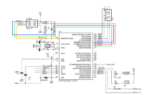
Now, in both cases, the official schematic and the KiCad schematic below, this subsystem grows to a size that is a little unwieldy to display on a web page, so I’ve shrunk it down to a semi thumbnail size. Make sure to click on it to expand it or download the full size so you can see it clearly. I’ve also tried to remove anything from the official schematic that is either already covered (USB, etc) or will be covered in future parts of the series (328P_DTR), so the schematic is a little different than the officially official one published, but we’ve already covered my problems with the published documentation.
The official schematic has connections on the left to the USB stuff, a crystal oscillator circuit, the supply voltages, and the In-Circuit Serial Programmer (ICSP) header. The right side has … well … whateverthehell JP2 is, the Data-Terminal-Read (DTR) line, some LEDs that flash when serial transactions occur, and the actual serial Tx/Rx connections to the 328P.
Interestingly, the right side of the schematic shows that there are a ton of pins that are absolutely and completely ignored. That’s a *lot* of capability just sitting there not just un-used and un-utilized, but effectively abandoned in place with no ability to access it.
As we’ve done in each part so far of the series, let’s take it step by step. We’ll start at the ICSP header and work our way counter clockwise (anticlockwise for all my English readers out there).
ATMEGA16U2 Subsystem Piece by Piece
ICSP Header
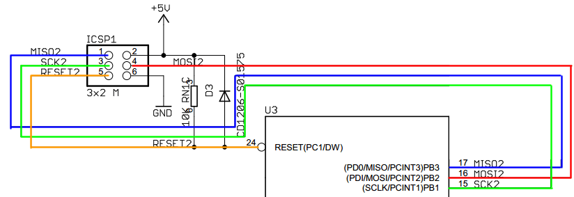
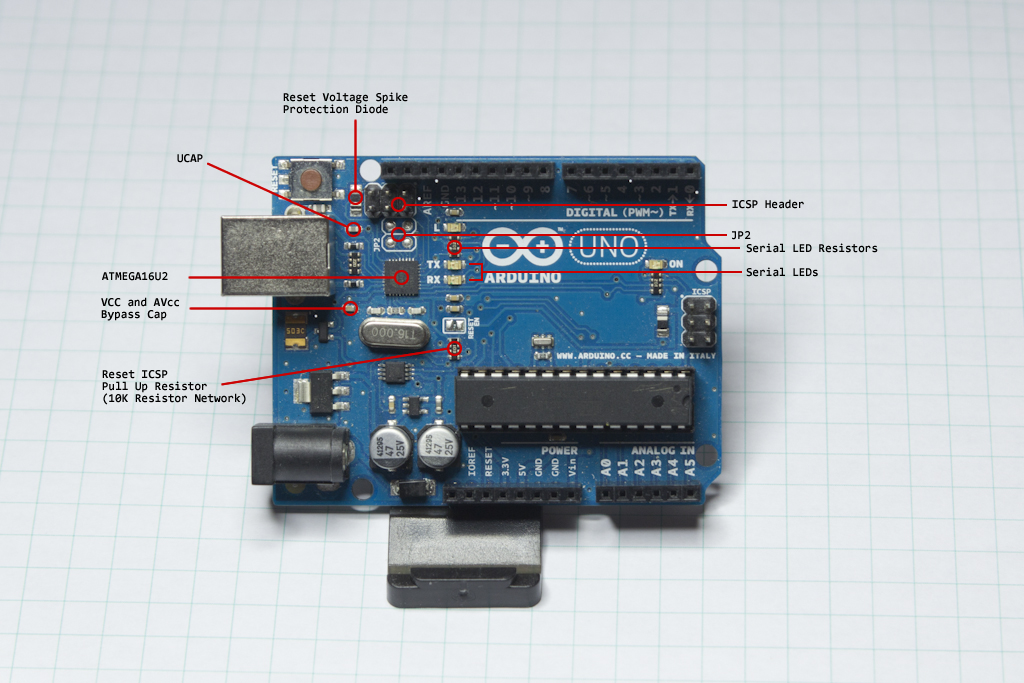
The In-Circuit Serial Programmer is the method that we will use to load firmware into our 16U2, using some form of AVR Programmer, since I sure don’t have a TQFN programming socket sitting around for these things. We’ll cover the way we actually use the header in the future, but right now, let’s look at the circuit.
You can see that we’re using the SCK / MISO / MOSI lines off the 16U2, the SPI pins. That’s where the “Serial” part of the ICSP comes in. Further, there’s a 5V connection, Ground and RESET. Reset is active low (which I denote here by using the overline macron, but on the Arduino schematic is shown by the circle at the base of the pin), so if and when the 16U2 detects that pin at a logical low state, it will process a system reset. The 10K resistor (RN1C) is there to act as a pull up resistor to 5V, creating a default “Not Reset” state for the pin. All of these pins are used in a specific sequence to set the micro into a specific programming state, then load code into it through the programmer.
The only thing left over to explain is the diode. It took a little digging to understand. It’s not common to find it on an ICSP header circuit, or if there is a diode, it’s used to prevent the programmer from inadvertently powering your project. In this case, it exists to prevent possible voltage spikes occurring on the RESET pin due to some exotic issue identified in the Arduino forums. As near as I can tell, it’s actually only a (potential) problem with the 328P, but it doesn’t really affect the circuit negatively, so they just duplicated that portion of the circuit onto the 16U2 as well.
For parts, I reused the same 10K resistor from the comparator subsystem voltage divider, and picked a Diodes Inc. 1N414BW-7-F spike protection diode, simply because there were more of them in stock at distributors than there were for the Bournes part listed on the schematic CD1206-S01575, and the Diode’s Inc. part is lower in risk. The actual physical header is just a really, really standard 0.1″ two row, six pin connector header. I picked a Harwin M20-9980346.
16Mhz Crystal Oscillator
Supply Voltage AVcc and Vcc
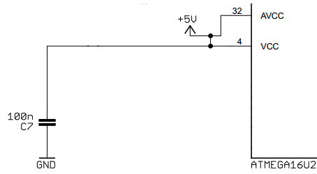
This is pretty simple, actually. Vcc is the connection that allows you to deliver voltage to the digital portions of the 16U2, like the digital GPIO ports. AVcc is the connection that allows you to deliver voltage to the analog portions of the 16U2, like the Analog-to-digital converters (ADCs). The datasheet (page 4) says you should connect AVcc to Vcc through a low pass filter, which helps to stabilize all the analog stuff the micro might do. Well, we’re not actually doing any analog stuff, so we can get away with just tying AVcc and Vcc together and use a single normal 0.1uF bypass cap.
USB Pins and GND
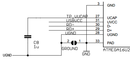
The D-, D+ and UGND pins all connect to their respective matching nets in the USB Connections Subsystem.
The UVCC pin, supplies a voltage regulator built into the 16U2, and is used exclusively for generating USB voltage levels. When USB is connected, we need to make sure this is as well, so that means making sure it gets tied to the USB_VCC net BEFORE the P-Channel MOSFET in the voltage comparator circuit, not after it.
The UCAP pin provides a place to connect the output cap for the internal USB regulator. According to the datasheet (page 5), it’s a 1uF cap. I’ll use the same type found on the input to the LP2985-33DBVR 3V3 regulator.
UGND is the USB ground pin and is tied to GND (figure 20-5 page 187). Arduino uses a weird solder jumperish looking thing that on the schematic looks like to half moons facing each other, and on the bottom of the PCB looks like to silver surface mount pads that are almost touching. I’ve used solder jumpers before, specifically to allow a user to disconnect the I2C pull up resistors on the AT30TS750A Temperature Sensor and MCP7940N Real Time Clock breakout boards. Frankly, they’re a pain in the doohickies to deal with, so I’ll use a 0 Ohm 0805 resistor instead.
The “33 PAD” pin, is the big ground pad that exists under the “Quad Flatpack No Lead” package (QFN). I’m not convinced I’ll use a TQFN instead of a QFP package that has actual pins you can solder to with an iron. For now, I’ll just keep with the original part designation and plan on the QFN.
Serial Lines and LEDs
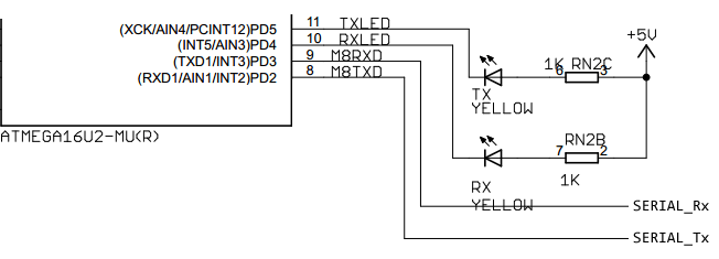
Again, this is pretty simple. The Serial Transmit pin (Tx) of the 16U2 is cross connected to the Serial Receive pin (Rx) of the 328P, and the Rx pin of the 16U2 is cross connected to the Tx pin of the 328P. The LEDs that blink during serial communications are on pins 10 and 11. They are connected to +5V, so somewhere in the USB to serial code, pins 11 and 10 are set as outputs and are driven to gnd to create a path for current to flow. That has to be handled all in the 16U2 firmware we’ll eventually upload.
DTR Net
This is just a net name, and will be investigated thoroughly when we put together the ATMEGA328P Subsystem.
JP2
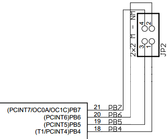
I have no idea what this is for. No clue. It seems to be the remains of something someone planned to do, but either never got around to finishing, or decided it wasn’t worth it. Instead of not connecting the pins, as is done with many others, they ran them out to plated through-hole (PTH) positions on the circuit board and those wind up getting filled during the wave solder process. It’s just bizarre. Useless and bizarre.
Arduino UNO R3 ATMEGA16U2 KiCad Schematic
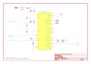
Here is the KiCad schematic for the ATMEGA16U2. It includes the full crystal oscillator circuit which, as I say below, will be covered in the very next post. I won’t publish the BOM yet, I’ll do that after we take care of the xtal in the next section. Again, it’s a little largish, so I’ve included the thumbnail here, which you can click to enlarge or download.
I just want to quickly point out the JP2 connector in the upper right hand corner of the schematic that is listed as “NO_POP”. That means “Not Populated” — no real component is going here. It will just be a footprint when we get to the PCB layout portion. I don’t know if I’ll make it a through hole footprint or a set of surface mount pads yet. I’ll figure that out when we get that far.
In Part 9, we’ll finish the ATMEGA16U2 Subsystem by looking at the crystal oscillator selection process.
