In Part 2 we dug into the voltage regulator subsystem. After thinking about it for a bit, I wasn’t happy with that schematic, and wanted to follow up with a revision that included new net names and included the power on LED that I didn’t have in the first one.
Build An Arduino UNO R3 from Scratch Table of Contents
Schematic Net Names
Net names, in a schematic, are a way you can annotate the actual connections between areas of your design. Just like you annotate the components, like calling a resistor “R1” or “R3”, you can label the nets to help you keep things straight.
I bring this up, because there are multiple different voltages zinging around the Arduino. There is a 5V USB connection, there is the potential for having an external voltage source connected to the barrel jack, you can supply voltage at the VIN pin, and you have the different voltages coming out of the LDO regulators. My key point for realizing that I needed to pay attention to this, involved working with the voltage management section (covered in the next post). I noticed there was a net named “VIN”, but realized I didn’t have a corresponding point in the LDO schematic, which didn’t make sense. Then there was the USB 5V rail, as opposed to the regulated 5V and I knew I had to bring order out of chaos.
Power Net Plan
Looking over the schematic, I’ve discovered that I need to list four nets to keep the voltage levels organized correctly.
- VIN: Variable voltage source originating from the barrel jack or the VIN pin header.
- USBVCC: 5V voltage source originating from the USB jack.
- 5V_LDO: 5V voltage source originating from the output of the LD1117S50TR 5V fixed voltage regulator.
- 3V3_LDO: 3.3V voltage source originating from the LP2985-33 3.3V fixed voltage regulator (covered in next post).
Now, when I add these voltage connections to the schematic, it will make sure that I do so correctly, and not cross connect anything like an idiot (because I am an idiot). If I just used “+5V” there is a solid chance I’d try connecting regulated 5V some place I should put USB 5V.
Revised Voltage Regulator Schematic
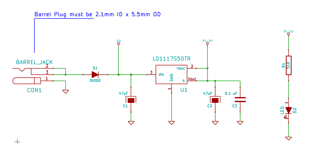
Here is the new Voltage Regulator Subsystem schematic.
The obvious change, is that I’ve added the Power On LED on the far right. This is as exceedingly simple as it gets… as soon as the output of the LD1117 exceeds the LED VFORWARD level with enough current, it will light up.
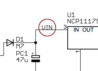
The less obvious change is the net names. I’ve added VIN to the input of the LDO, and added 5V_LDO to the output. This will make sure that the correct voltage rails go where they’re supposed to go.
Now, I wasn’t sure based on the official schematic, if VIN should go before or after the protection diode. I used my multimeter and checked by toning out the signal path (you older telco guys will know what I mean by “toning out the line”) from the VIN pin header to pin 3 of the LDO, confirming that as a valid connection. That means that it comes after the diode, because I wouldn’t have been reading 0 Ohms if there was a diode in the way, my multimeter would have shown the VFORWARD for the diode instead.
Here is the new BOM including the power on LED section…
BOM (csv): Arduino UNO R3 Clone From Scratch – Voltage Regulation Subsystem v2
