With the release of the new officially stable version of KiCad, many improvements have been brought to us the faithful users, but some of those changes represent a hard break with the previous stable version, BZR_4022. My entire business runs on KiCad being a complete reliability afterthought, so making the tiny steps across the nightly builds wasn’t going to happen. My upgrade had to wait until there was a release that locked down features and was in pure bug fix mode. Version 4.0.0_RC1 is exactly that.
Those fundamental differences between the two versions, BZR_4022 (the old stable) and v4.0.0_RC1 (the new stable) present challenges depending on your location in the design development cycle. This post will help you import an old kicad project from the old stable version into the new stable version.
A Completed Design
If you have a completed design, and only need to use the schematic and PCB layout as references, then you won’t have any trouble at all using the new stable version. The layout, in particular, just opens up as you would expect — there aren’t any weird artifacts that show up, or traces that suddenly bend in Lovecraftian dimensions. Your schematic will require a little massaging using an automatic “component rescue” tool, that takes components in your drawing that miss direct matches in the new version, and loads them into a project specific library associated with your project called %project%-rescue. You’ll also probably see an error message saying the “Special Library Not Found”, which isn’t a big deal. The main problem is that the associations between your schematic and your PCB effectively no longer exist, so, like I said, they are both reference documents. As long as you never need to have a modification flow from one into the other, you’re cool.
Completed/In Progress Schematic but No PCB Layout
Again, if you haven’t done any PCB layout yet, then the new method of footprint association won’t hang you up, because you don’t have any yet. Opening up your schematic in the new version of EESCHEMA will still require the component rescue tool to run, and create the %project%-rescue file, but that’s not a big deal. It’s up to you if you want to go back and replace all the components that don’t match with new ones, but considering it will be essentially every passive on your board, I’d say it’s unlikely, because that would be a lot of metadata to retype!! (You are storing all your component information in your schematic right!??) In the end, you’ll just use CVPCB, save the netlist, import into PCBNEW and go down the merry road without issue.
In the middle of PCB Layout
This is where the problem lies, and the main subject of this post. You’re either designing the schematic and layout one subsystem at a time, or you’ve got an isolated glob of modules off to one side you draw from when you’re ready to move onto the next section. There are going to be changes, particularly after you get the first prototype back, and you must have the flexibility to make changes in the schematic that will flow through to the PCB: net names, components, connections, you name it.
Previously, in BZR_4022, the association between your schematic and your layout footprints lived in a file called %project%.cmp, that you created in CVPCB. You still use CVPCB to create associations in v4.0.0_RC1, but there is no CMP file, the associations just get loaded into the “FOOTPRINT” field of every component in your schematic, which is good because that’s where *all* component information should live. You then generate a netlist which contains those footprint values and that’s what PCBNEW works with. In BZR_4022, who cared if you ever back-filled the footprints into your schematic; in V4_RC1, it’s happening regardless.
10 Steps to Import an Old KiCad Project into v4.0.0_RC1
Step One
Things to Consider and Prep Work
It is absolutely critical that BEFORE you open any old projects in the new version, that you recreate any custom component property fields in EESCHEMA that you created in the old version, so the values will transfer over. If you don’t, those values are lost irrevocably.
If at all possible, try to install / run the two versions in parallel, so that you can grab some information from the old version to import into the new version. Also, consider creating a subfolder called “V4_IMPORTED” or something like that, and copy the project directories you’re working with into it wholesale, so you can work in both versions side by side. When you’re done importing, you can delete the old project versions without worry, or move it to long term offline backup.
Step Two
Open the schematic in EESCHEMA and allow it to create the %project%-rescue library for all the components it can’t find a match for. This could get ugly because it’s going to do that with pretty much everything. Let it do what it needs to do. Then save and close EESCHEMA.
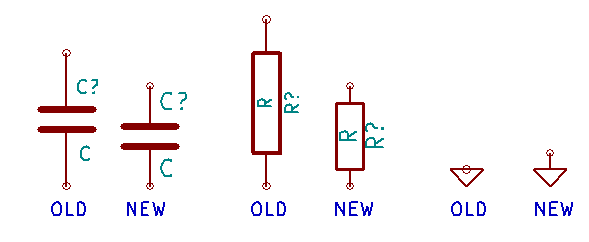
This doesn’t really affect your transfer of footprint associations between EESCHEMA and PCBNEW, it’s just the first step to bringing an old project into the new version. As I say above, depending on the complexity of your project, you can go through and replace all the old style components with new ones, but that might be a tedious process. Your caps and resistors may end up a little funny looking in some of your designs, but so what — it happens.
Step Three
Open PCBNEW and reconnect all the custom libraries that were associated with the project in BZR_4022 – those associations don’t translate into the new version. When you add them, select the library “Legacy” Plugin type. When you’re done, save and close PCBNEW.
This is where opening the old copy of the project in the BZR_4022 while still running the new stable release is handy. If you are able to do so, go into the old version and note the names and locations of all the old custom libraries in notepad or equivalent text editor — unfortunately you can’t copy the path and file name, you’ll have to type it manually. When you’ve got all that ready to go, use the Footprint Libraries Manager in the new version of PCBNEW to add all of those libraries as Project Specific Libraries.
If your install of v4 overwrote the old version, then your best bet is to go into PCBNEW and have a look at everything in there and make a note of any custom footprints you might have created. I’m guessing all of us wind up with some sort of standardized way of managing our custom libraries, either with a single folder that has everything in it, or a project specific one in each project folder, but you’ll need to hunt all of those down and do the association in the Libraries Manager, before you can go any further.
Step Four
Open EESCHEMA, and bring in your footprints using the footprint “back import” tool, using the old CMP file created with CVPCB back in BZR_4022. You may never have done the footprint retro-import before, because it really didn’t serve much of a purpose in old stable, but now the schematic is the master resource for all footprint association data. When you’re done loading the footprint values, save EESCHEMA but leave it open.
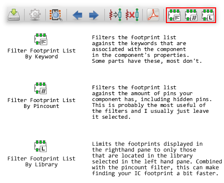
Even though the new version of KiCad doesn’t create or modify the CMP file any longer, EESCHEMA still retains the ability to import the CMP stored footprint values into your schematic. It’s the funky little “BACK” icon all the way to the right on the toolbar. Normally the CMP file should be in the project folder along with all the other project files.
Step Five
Run CVPCB from within EESCHEMA. You’ll receive the “some of the assigned footprints are legacy entries” message. Click “yes” to have CVPCB convert them to the new naming convention. This is why you had to re-associate all the libraries up in step 2 — so it wouldn’t have a problem with any of your custom footprint parts. Where it will stumble, though, is on actual KiCad default library footprints you previously used. Leave CVPCB open.
CVPCB is no longer a stand alone application, but a sub-utility within EESCHEMA, and is accessed from an icon on the toolbar, up by NETLIST and BOM.
The new footprint association has a new naming standard. Or rather, there is now a naming convention — %library_name%:%footprint_name%. This is ultimately what you’re trying to drive into your component footprint fields in EESCHEMA, and ultimately what PCBNEW will expect to find when it opens the netlist file. If the footprint doesn’t follow that convention, the association between component and footprint is lost. As an example, the BZR_4022 footprint field would have been populated with “header_100mil_5x1”; now it’s “100mil_headers:header_100mil_5x1”.
(That is a custom 100mil pin header library I made after having selecting mechanical pin header footprints rather than normal pin header footprints, thus rendering a whole batch of prototypes unusable.)
You have to do this step, so that CVPCB can use those footprint names to try to create the new associations in the next step.
Step Six
You now go through all the components in CVPCB that didn’t receive the “library:component” association, and select appropriate footprints for them – essentially, anything that you used a default library footprint for. On the positive side, at least you’ll start figure out where all the passives are 🙂 When you’re done, save and close CVPCB.
I certainly hope I’m missing something, and I actively welcome anyone with greater knowledge than I of the new version (there are a lot of people that know more than I about pretty much everything) to tell me how to do this more efficiently. It strikes me as odd that the footprint associations just can’t carry over, or somehow be automatically reconnected. Maybe the developers decided that a clean break had to be made with the past.
Regardless of the reason, and failing any other means, this is the most tedious part of the whole process, at least for the first few projects you’ll do. There are an absolute maze of new libraries that it’s sucking out of GitHub, and I’m not entirely confident with which ones are which and contain which things to be able to tell you that you can unload 90% of them as Global Libraries in the Footprint Libraries Manager. You’ll start to figure out where things are and as you do, you’ll get faster at this (as you did with the old version of CVPCB). There are a few tricks that can help.
First, before you even begin any of this crap, you can view the new footprint libraries and their contents by opening the new stable KiCad Manager application, selecting the PCB Footprint Editor application, and then opening the Footprint Viewer from within the editor. It’s going to load up all the GitHub stuff, so be patient with it.
Second, passives have their own libraries, so if you’re working with inductors or diodes or resistors, whatever, select those as the library in the left pane, and you’ll see the footprint in the right pane, and make the selection in the middle. Most standardized IC footprints are now located in a section of libraries called “Housings_****”, with **** giving you an indication of what is inside. There is also an SMD_Packages library that has a bunch of unsorted BGA, SMD passives, SSOP, SOIC and the like in it as well.
Finally, get used to using the filtering buttons within CVPCB.
The end result, after you save and close CVPCB, will be all those new footprint associations overwriting the values that were originally in your component footprint properties.
If you don’t want to bring a set of component into your PCB yet, just leave the association blank. Be careful though because you can’t make a component “un-associated”. Once an association is set, you can only change it to another footprint. The only delete capability you have is to delete every association and start building from scratch in CVPCB. I cannot fathom why a line item delete wasn’t added.
Step Seven
Generate a new netlist in EESCHEMA.
Generating the netlist is the final step necessary prior to opening your layout in PCBNEW. This will bring together all your connections, components, nets, footprints, pins, all that stuff. This acts generally as it did in BZR_4022, even though what it does behind the scenes is different.
Step Eight
Read the new netlist into PCBNEW. You’ll get a scary message saying “What you are about to do cannot be undone”, as though you’re about to throw The One Ring into Mount Doom. Chuckle at this error message and click “Yes”.
As it processes the netlist, you’ll see a lot of soft errors show up during this process reporting a mismatch between what is in the netlist file, “library:component”, and what is already on the board, “component”. That’s fine – it just means PCBNEW realizes those parts are taken care of. What it won’t do, is repopulate your board with a bunch of duplicate components that you have to clean up. This is just the confirmation that you have assigned the new footprint to the component, but an existing footprint is already there, so it’s skipping it.
NOTE: If you delete any of your existing components from the board and then read the netlist in again, it will be replaced by the new footprint.
Step Nine
Just to be safe, run DRC and see if all the tolerances and connections actually loaded right.
All your DRC rules and presets should have transferred over, like minimum trace widths, via sizes, custom trace widths, solder mask tolerances… all of that. The DRC should take all of that into account and you shouldn’t see anything that surprises you. Obviously, if you do have that blob of components waiting to be laid out, you’ll get a lot of disconnect warnings but what is already placed, shouldn’t evaluate in DRC any different than it would have before.
Step Ten
Save Everything.
Just go into EESCHEMA and PCBNEW and save everything so that your changes are committed, just in case they weren’t before.
That’s it! You’re done! At this point your project is v4.0.0_RC1 compliant, so you can delete / archive the BZR_4022 version, and you’re ready to start modifying your design within the new version of KiCad at will.
You can test it quickly by…
- Dropping a resistor into your schematic and hitting both ends with “Not Connected” flags (blue x’s).
- Go into CVPCB and associate it with some relevant footprint.
- Save CVPCB and go back into EESCHEMA and save the NETLIST.
- Go into PCBNEW and load up the new NETLIST and make sure the new resistor shows up with no associated ratsnest.
For more KiCad tutorials, Click Here.
