Just as we did for the I2C signal, we’re going to pull a SPI signal apart using an oscilloscope. Because of the wide variety of configuration possibilities, reading the signal requires greater research into the components involved up front.
Objectives
- Determine what information you need to know before attempting to interpret data
- Identify the SPI Mode based on the actual CPOL and CPHA
- Determine the value in binary and hex of the data being sent and returned
Background
SPI Basics
SPI Signals
Schematic
No schematic is associated with this module.
Setup
The goal of this module is to focus on the signal itself, rather than on the hardware, however this module can be replicated in its methods by using a four channel oscilloscope capable of reading a 4Mhz signal connected to the CS, SCK, MOSI and MISO lines between an Arduino and any SPI chip. A two channel scope can be used, by triggering on a falling CS edge and then working with each of the other three channels in turn.
SPI Signal Reverse Engineering
SPI signals are much more simple than I2C. There are no start and stop conditions to evaluate, no repeated starts, no ACKs or NACKs. However, because the parameters that involve the creation of the SPI signal are so loose, you need to know a bit more about what to expect before going in. That means grabbing the datasheet of the chip (or chips) in question and doing a bit of research to understand the possible interactions.
The first thing you’ll want to do, is determine which chip you’re working with. As each SPI device typically has a discrete connection to it’s CS pin, it’s relatively easy to work along the micro and find the signal that is being toggled to control the low going signal that starts the interaction, then power off the board and check for conductivity between that pin on the micro, and the CS pin on each of the SPI components. One of them will most likely tone out as the connection. For the purposes of our test here, you should be able to use your multimeter to verify a connection between Digital4 of your Arduino, and pin 10 of the MCP3008.
The next step is to go and grab the datasheet for the chip in question, in our case, we’ll be working with the MCP3008.
Refer to the datasheet and answer the following questions…
What is the expected bit order?
Hover mouse to read answer
What is the fastest allowable speed?
Hover mouse to read answer
What are the acceptable SPI Modes?
Hover mouse to read answer
SPI Signal Overview
Without going into the full details of how you need to interact with the MCP3008 in order to receive valid data (and we’ll just assume that the code we’re receiving the end result of is, in fact, doing just that), with the above three configuration parameters, we can start to make sense of what it is that we’re receiving.
Here is the overview of the communication. Zooming all the way out on the signal showed that more than 100ms passed in between signal captures, and each of the signal captures looked essentially identical, so it’s reasonable to assume that we’re capturing the sum total of the interaction with the chip.
The scope was set to trigger on the falling edge of the CS pin, and as you can see, it appears to have captured three bytes of data.
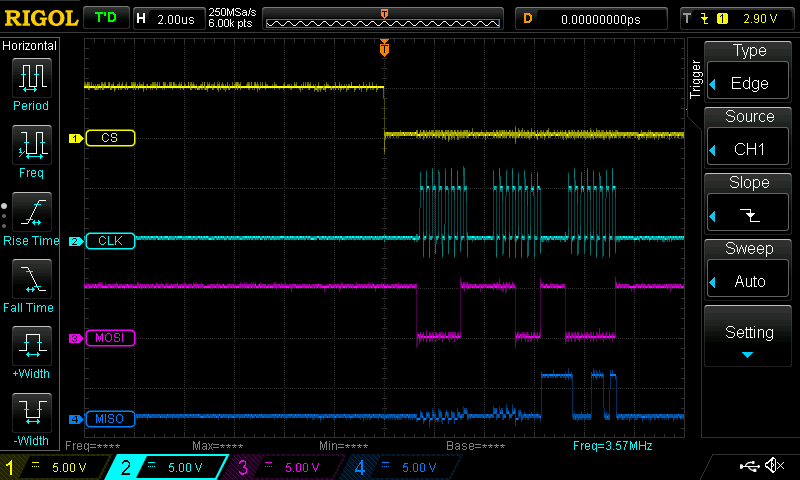
By zooming in a little and adjusting the time domain we can see the full interaction from CS going low, indicating that we’re going to do something SPI-ish with the chip. (The one thing I didn’t think to do was capture the full interaction to show CS going high after the third byte, so you’ll just have to trust me that it does 🙂 )
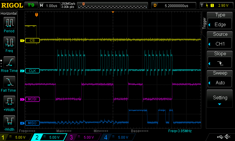
Before going any deeper into the signal, we can immediately tell that the clock polarity, CPOL, must be 0, because the clock is in a logic low state prior to CS going low. From the research, we know that the only two accepted SPI Modes were MODE0 and MODE3, and since CPOL is 0, then we’re in MODE0. That mode also indicates a CPHA of 0, so we can infer that data will be sampled on the rising edges of the clock, and transitions will occur on the falling edges.
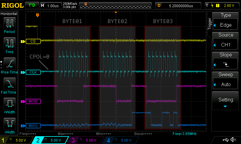
You can also see in the lower right hand corner that the scope is measuring a clock frequency of 3.85Mhz, which is faster than I should have selected the speed, as the preferred clock speed according to the datasheet is a max 3.6Mhz at VDD of 5V. Oops.
SPI Signal Byte 01
Knowing that we have three bytes to work with, we’ll zoom in on the first byte. Here is the byte without the overlay…
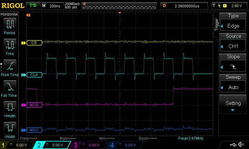
And here it is with a little bit of overlaid graphics to help explain what’s going on…
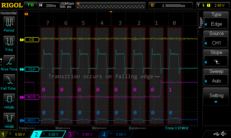
As expected we can see the transition of the MOSI line is happening on the falling edge of the clock pulse, which means the rising edge is where we’ll determine the bit of data being transmitted. The datasheet indicated that data is sent MSB first, so that’s how we’ll have to interpret the values we’re seeing. This first byte doesn’t show much activity though, with 0x01 appearing on MOSI and 0x00 appearing on MISO.
SPI Signal Byte 02
This is the second byte without the overlay…
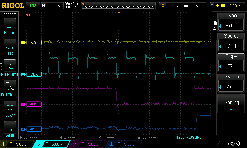
…and with the overlay…
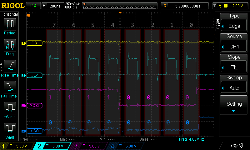
Looking at the rising edge of the clock pulses to determine the values being sent, we can read 0xF0 off the MOSI line and another bunch of zeros on the MISO line. So far all that has occurred is a single bit being written in the first byte of data and then B11110000 being written in the second. In neither case has the chip we’re working with responded with anything yet.
SPI Signal Byte 03
Our final byte of data on the SPI bus shows a little more activity now…
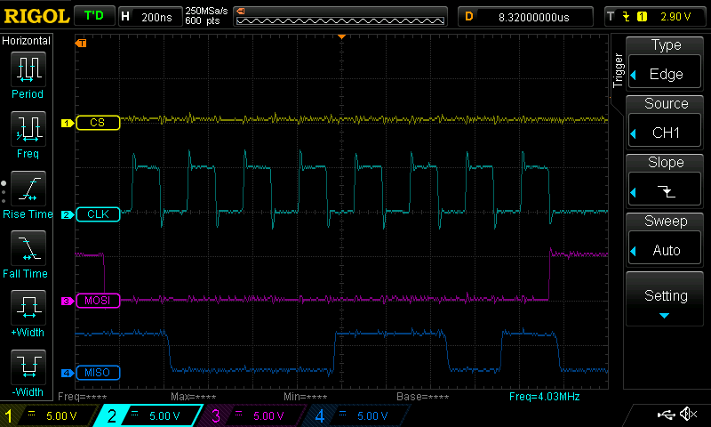
…and again, with the overlay…
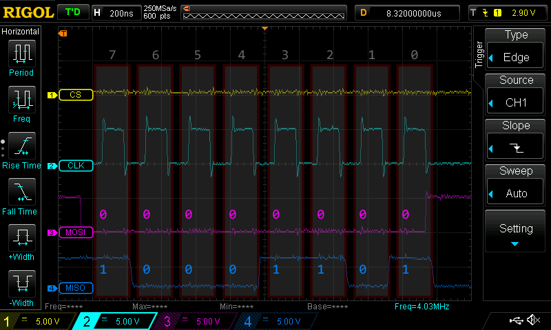
MOSI is writing a bunch of zeros to the line, but MISO is responding with 0x8D. After this byte of data, the CS went high, so this is the end of the full interaction with the chip.
SPI Signal Summary
Here is what we saw broken down by byte…
| Byte Number | MOSI Value | MISO Value |
|---|---|---|
| 01 | 0x01 | 0x00 |
| 02 | 0xF0 | 0x00 |
| 03 | 0x00 | 0x8D |
If you go through the full datasheet to understand the interaction, we’re sending a start bit to tell the MCP3008 to prepare to perform a sample, that’s byte 01. Then in byte 02, we’re telling the ADC what we want to measure, 0xF0 being a single ended measurement of ADC Channel 7. One clock cycle later, the ADC will have completed the measurement and begin providing the output, however, since we see all zeros, the measured voltage level must be closer to 0V than to 5V (because I have the 5V VREF selected). In byte 03, MOSI is all zeros, because the code is sending a junk value as necessary, but the 0x8D value on MISO, decimal 141, is our digital equivalent of the analog voltage level. Using the formula from the datasheet, that means we are measuring 0.688V.
I must have had that potentiometer screwed all the way down!
