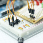
In this tutorial, we’ll start to explore how to interact with the I2C Display Add-on using the I2C interface of an Arduino. The Display features a four digit seven-segment display as well as two bar graphs made with red / green LEDs all driven by an AMS AS1115 Display Driver. The register map for the driver is quite extensive so we’ll need to dig into the configurations to see what’s possible.
Background
I2C Basics
Changing the I2C Library
AS1115 Datasheet
I2C Display Setup
The Display only requires six connections: 5V, GND, SCL, SDA as well as a connection for the multiplexer and the piezo speaker. It was designed to work directly with the I2C and SPI Education Shield, and as because of that, it does not have I2C pull up resistors on board. Depending on what you’re connecting to, it may be necessary to provide those resistors as well as series resistors on the SCL and SDA connections. For general connections to an Arduino or other development board, pull up resistors of 4.7K should be sufficient. If you need to use series resistors, 100Ω is fine.
AS1115 Display Driver Overview
The brains of the I2C Display is the AMS AS1115 display driver, and it provides all the LED power and signal processing necessary to turn the LEDs on and off. One of the distinct advantages of this IC over others, is that it has built in functionality for displaying human readable alphanumeric values on the seven segment display, which means you don’t have to store a bunch of character maps, but also provides the ability to turn that decoding off so you can manipulate LEDs independently. It’s quite a powerful little chip. Let’s look at the features in depth.
Digit Register
The primary design of the chip is to control seven segment displays, and consequently, banks of eight LEDs are controlled as “digits”. In a seven segment display, those eight LEDs are typically configured (and referenced) in this pattern…
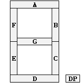
The seven bars of the numeral plus the decimal point add up to the eight LED segments in each digit.
The digits are referenced in the datasheet as Digit 0 through Digit 7, with corresponding register addresses of 0x01 through 0x08.
Brightness
Brightness of the display as a whole or of individual digits is controlled using the Global Intensity Register 0x0A and the Digit Intensity Registers 0x10 through 0x13.
The brightness value is a scale from 0-16 with 0 being dimmest and 16 being brightest. Obviously how “bright”, bright actually is will be entirely subjective, so you’ll have to play around with it to determine what’s best for the environment you’re using the display in. From my experience, intensity level of 16 is really bright, and pretty current thirsty.
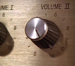
You set the global brightness by applying the 0-16 value to the 0x0A register, which will ignore the most significant four bits, so only values of 0x00 through 0x0F should be used. The four individual digit intensity registers follow the same 0-16 level, but each register uses the lower nibble for one digit and the upper nibble for the next.
| Upper Nibble | Lower Nibble | |
|---|---|---|
| 0x10 | Digit 1 | Digit 0 |
| 0x11 | Digit 3 | Digit 2 |
| 0x12 | Digit 5 | Digit 4 |
| 0x13 | Digit 7 | Digit 6 |
Decode Enable
As mentioned above, the AS1115 already knows what certain alphanumeric patterns look like, and consequently, you can set a digit to be decoded in that fashion. Alternatively, if you so choose, you can turn decoding off and reference each individual LED discretely. This can all be configured on a digit by digit basis, which is what enables the bar graph to function in a linear fashion, and the seven segment display to be easily programmed simultaneously. There are two different decoding methods: Code-B Font and Hex Font, and you have to select one or the other globally by setting the Code-B / Hex bit, bit 3, in the Feature Register, 0x0E.
By adding a single bit in the fourth bit position, you will enable the decimal place for any of the characters in either font format.
If you choose not to decode, then each segment is treated as a discrete LED. On the I2C Display, the bar graph LEDs are configured left to right exactly as you see in that graphic.
After selecting which decoding system to use, you then disable/enable each digit for decoding by manipulating the Decode Enable Register, 0x09. Each digit will decode as to the selected font mapping, if you set it’s respective bit. If you clear it’s respective bit, the segments will be treated as individual LEDs.
Digit Enable
The Scan Limit Register 0x0B is used to select which of the digits are displayed. However, since this is designed to work with an eight digit display, configured 7 to 0, its usefulness for the I2C Display is negligible. You can write the values 0-8 to this register to enable another digit in turn: 0x00 = Enable Digit 0, 0x01 = Enable Digit 0 and 1, 0x02 = Enable Digit 0, 1 and 2, etc.
Shutdown Modes
There are four different power states for the AS1115 controlled with the Shutdown Register 0x0C. those power states correspond to the following values sent to the Shutdown Register…
- 0x00 = shutdown to minimal current draw, display disabled, feature register reset.
- 0x80 = shutdown to minimal current draw, display disabled, feature register preserved.
- 0x01 = full functionality available, display enabled, feature register reset.
- 0x81 = full functionality available, display enabled, feature register preserved.
How you move in and out of the shutdown modes will determine the extent to which you reset the device.
AS1115 Display Driver Feature Register
The Feature Register 0x0E covers additional operating characteristics of the AS1115 not directly associated with telling it what value to display or how bright to display it.
Bit 0: External Clock Enable
This bit is used to allow a designer to use the I2C clock pin of the circuit as the system clock for the chip. This configuration isn’t supported on the I2C Display so leave this bit cleared (default state).
Bit 1: Software Reset
My interpretation of the datasheet is that if you set this bit, it should revert all of the control registers back to their power up default values, however that is not the case in practice. I haven’t been able to figure out what this bit actually does, and have sent a message to the manufacturer asking for clarification. I’ll update this as I learn more.
Bit 2: Decode Select
Determines globally, whether to decode using the Code-B Font or Hex Font. Leave the bit clear for Code-B, set the bit for Hex.
Bit 3: Not Used
This bit isn’t used and is not evaluated by the chip.
Bit 4: Blink Enable
This does just what it sounds like, causes the entire display to blink at the frequency specified in Bit 5.
Bit 5: Blink Frequency
Provided you are using the internal oscillator, this will cause the blink to be either .5s on / .5s off (bit cleared) or 1s on / 1s off (bit set).
Bit 6: Blink Synch
This would cause the blink cycle to begin on the rising edge of the LD/CS pin. However, there is no LD/CS pin so I’m not sure why this is listed in the datasheet. Again, waiting for clarification from the manufacturer, but I suspect this is a generic entry left over from documentation on the SPI enabled brother of this chip that has an actual chip select pin, and the rising edge of that pin (meaning the end of a SPI interaction) would cause the display to start blinking. Do this across a bunch of devices at once and you synch all their blinking.
Bit 7: Blink Start
Determines if blinking starts when the display is turned on or when the display is turned off. This can also be used as a way to synchronize blinking.


