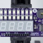
The Rheingold Heavy Education Shield is my response to a problem I discovered as I was pulling myself up by the bootstraps in electronics. There are a million starter kits out there: LEDs, photo resistors, motors, servos and a handful of passive components designed to get you up and doing something – anything – with electronics. But once you go through the dozen or so tutorials, you’re left with a breadboard connected to a single cheap servo, and you know how to digitalWrite(ledPin, HIGH) . I worked diligently with it, but I wanted more — I wanted the next step. That’s when I developed the idea for the I2C and SPI Education Shield.
As I show in the July Build Log for the I2C and SPI Education Shield, I settled on this as the design requirement: build an Arduino shield with a variety of I2C and SPI modules that allow a user to practice developing against those data transfer methods. That design had to meet 10 goals…
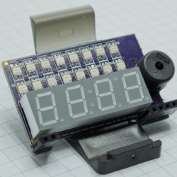
- Interface with an Arduino Uno R3
- Multiple modules for each communication method to allow working with CS, etc.
- Make it do something useful, so it has long term value.
- Exquisite documentation.
- Use a shift register to bring the very basics of serial communication to the board.
- Include modules that require both read and write.
- Make it expandable with sockets, headers, terminal blocks, breadboard connections, etc.
- Offer components that allow it to be used as a kit with accompanying documentation.
- Aim for a specific price range, shipped, of around $100.
- Ensure ease of assembly and testing for production.
To meet these goals, I developed six modules that are accessible on the board.
- A manually controllable shift register circuit. Shift bits with your finger tips!
- Three tactile buttons, debounced with hardware.
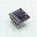
- A temperature sensor with an I2C interface.
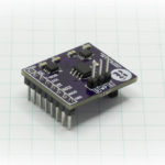
- A real time clock with an I2C interface.
- A 10-bit 8-channel analog-to-digital converter with a SPI interface.
- 8 Mbits of Flash memory
Now the first prototype has been completed! All those teeny surface mount components were all hand-soldered by yours truly! It’s not without it’s flaws, so I’ll need to respin the board after doing some design revisions, but I think this is exactly the sort of learning tool I was looking for once I set down my LEDs and thought, “well now what?”
The centerpiece of the board, is the absolute basics of serial communication, a 74HC595 shift register, with three hardware debounced buttons connected to CLOCK, LATCH and DATA. I figure the more that electronics can be demystified, the easier it is to learn it, and what better way than by clocking zero’s and one’s by hand, mechanically. There are three jumpers at the top of the board, so that the buttons can be decoupled from the shift register, and allow it to be controlled programmatically… what better way of understanding bitwise operators than to be able to visualize 0xD1 | 0x2E.
The I2C temperature sensor is the least complex in terms of interaction, and that’s where the coding will really start, getting a handle on how to generate a clock signal, send and receive data using only two wires, and what that means in terms of benefits and drawbacks.
[masterslider id=8]
The Real Time Clock is an I2C component that is an order of magnitude more complex than the temp sensor, and a lot of time can be spent in there building alarms, interrupts, reading and writing to the time stamp and working with the battery backup subsystem.
The ADC is the first foray in the world of SPI (c’mon, it’s pronounced “spy” not S. P. I.), and I found about as simple an ADC as there is… no waiting for data ready pins, no clear or enable or whatever pins, just a simple 10-bit ADC that happens to be just as good as, and works right along with, the four ADC pins already on the Arduino (you weren’t counting A4 and A5 were you? Those are I2C as far as we’re concerned!) Once you get the little bit of setup out of the way, all it takes are five lines of code to get this thing reading back to you. I also included a jumper here to switch between a voltage reference of 5V and 3.3V. Neat!
Finally, there is the 8Mbit Flash Memory array. Because what’s the use of having all this other stuff, like the ability to read 8 analog sensors + temperature and slap a time stamp on it if you don’t have anywhere to log it! And just like the RTC was a step up in complexity over the temperature sensor, the memory IC is that much more intricate communication wise than the ADC.
For my part, I consider this project only half down with a completed production board. It needs solid documentation to go with it (Design Goal #4), so now that the “let’s see if I can make this work” part is done, I’ll get started with preparing sumptuously detailed documentation to go with it. Hopefully, I’ll have an opportunity to put one of these in your hands soon!
Update 19-AUG 2014! Rev. 1 has been submitted for fabrication!
[masterslider id=10]
Update 07-SEP 2014! I received the Rev. 1 boards back and the new components and it’s fully assembled and functioning. Only one critical design modification is needed, the ground pad for the battery holder needs to be increased in size to ensure good contact with the battery, but I won’t need to respin the board for that. All the chips are functioning as expected, the board is good to go!
[masterslider id=9]
