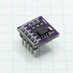
Welcome to the AT25SF081 8-Mbit Flash Memory Device from Adesto Technologies. This module will cover the read, program and erase functionality of the chip based on the datasheet. If you weren’t comfortable with reading hexadecimal values before, you will by the time you’re done with this!
Objectives
- Define what a Megabit is.
- Understand what is meant by “Random Access” memory, rather than sequential access.
- Understand what is meant by “endurance”.
- Determine the memory address locations.
- Understand how to read the array.
- Understand the different program methods.
- Understand the different erase methods.
Background
Decimal, Binary and Hexadecimal Number Systems
SPI Signals
How To Read A Datasheet
Adesto AT25SF081 Datasheet
Schematic
Education Shield – AT25SF081 Flash Memory Subsystem
Setup
There is no setup required for this module.
AT25SF081 Functionality Overview
The Adesto Technologies AT25SF081 is an 8-Mbit Flash Memory module. The memory is a series of registers, no different than any others that we’ve dealt with so far. The registers are arranged into groups of 256 bytes called pages, and there are 4096 pages. That means there are 1,048,320 bytes of memory, with 8 bits per byte = 8,386,560 bits… 8 megabits.
Each individual byte is accessible from a read or write command discretely. If you choose to start writing to a byte somewhere in the middle of the 1073 page, that is your choice, and you can write up to 256 bytes at a time. You can also choose to start reading from anywhere you want and just stream back as many bytes in a row as you need. If you get to the end of the memory array, it will just wrap to the beginning and read from there. This ability to read and write to any byte at random is why it’s called “random access” memory.
The erase functionality also allows you to start erasing from any point in the memory array, however you must erase not just the starting byte but in blocks of 4K, 32K or 64K bytes. The entire chip can be erased as well using a single command.
The good news is that anything you write the chip is non-volatile. It will survive power down and up cycles, and and as long as you don’t erase or overwrite those bytes, the chip will retain that data for 20 years.
The bad news is that each block has an endurance of 100,000 Write/Erase cycles before it must be considered “unreliable”, referred to as “Program/Erase” or “P/E” cycles. If you think “wow, a hundred thousand erase cycles for every 4K block, that’s a lot!”, think how fast we were able to query the MCP3008 ADC, 50K+ samples per second. If your code is just let loose in the main loop on the chip, you can rapidly blow through that 100,000 limit in short order. So we’ll have to be careful. For more information on the P/E cycle, read this article.
Memory Array Addressing and Organization
The full set of memory array bytes are located from 0x000000 to 0x0FFFFF. 0x0FFFFF in decimal is 1,048,575, meaning that’s how many bytes there are (and of course 8 bits in each byte means 8 megabits).
From a Read perspective, you can enter that array of one million bytes anywhere you want, and ready however many you want for however long you want. Read is entirely flexible.
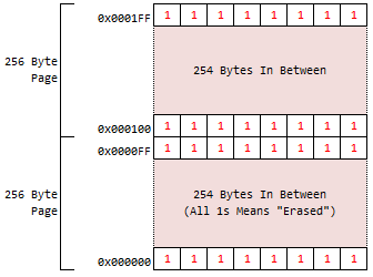
From a Write perspective, each of those bytes are arranged into groups of 256 bytes called “pages”, and you can fill anywhere from a single byte up to a full page with a write command.
From an Erase perspective, each of the bytes is arranged into a series of blocks, either 4000, 32000 or 64000 bytes to a block. The block erase command erases full blocks from the start of the block to the end of the block.

SPI Configuration, Operation and Configuration
The AT25SF081 is, as you may have guessed, a SPI controlled device. It supports data modes 0 and 3, and is transfers data Most Significant Bit first, so it is directly compatible with the MCP3008 ADC that exists with it on the SPI bus of the I2C and SPI Education Shield. It supports clock speeds of up to 104Mhz depending on the method used to read the data from the chip. Since the Arduino won’t function faster than 8Mhz, I think we’re cool.
There are seven main areas of operation within the AT25SF081.
- Read Commands: retrieving data previously stored in the memory array
- Program Commands: writing data to the memory array
- Erase Commands: erasing data previously written to the memory array
- Security Registers: three pages of isolated memory to be used for storing things like serial numbers, etc.
- Status Registers: contains information about the status of data protection, device ready/busy state, etc.
- Data Protection: write protection to prevent overwrite of existing data
- Miscellaneous Functions: contains the Manufacturers ID, Device ID, and the deep power down / up register
All interaction with the memory module begins by bringing the CS pin low and sending an operations code, opcode , to the device over the SPI bus. The opcode tells the chip what you intend to do: read, program, erase, read/write status registers, etc. For the memory array operations, the opcode is followed by the 24bit address that you want to start with. At that point you would start to receive data or send data, or wait until an erase cycle completes.
AT25SF081 Read Commands
The AT25SF081 is capable of single, dual and quad read operations, meaning you can output the data across up to four pins for rapid access. This feature is unavailable on the I2C and SPI Education Shield because the pins are not connected in a fashion that allows it (there weren’t enough digital pins remaining to support that sort of design), so you’re limited to single read operations. The AT25SF081 Breakout Board does support this feature as you can configure the pins however you like.
Of the single pin read options available you can read at up to 70Mhz clock speed using the 0x0B opcode or up to 50Mhz clock speed using the 0x03 opcode. Either are perfectly fine for use with the Arduino, because our maximum clock speed is nowhere near that fast.

With CS brought low, you send out the opcode during which the MISO line remains in a Hi-Z state. After that is transmitted, 24 memory address bits are transmitted from 0x000000 to 0x0FFFFF to indicate which byte of data will be the starting point of the read operation. If you use the 0x0B opcode, you then clock in a JUNK byte, and then data starts to return on MISO. Bytes will be transferred sequentially up to the final byte, at which point the data output will wrap around to the start of the memory array and continue indefinitely. You can raise CS at any time to end the transfer.
AT25SF081 Program Commands
Data can be written to any byte location that has been erased; you cannot overwrite data already present. A location is considered erased if all the bits are set to 1, 0xFF. Before you can begin any write operation, you have to set the Write Enable Bit (referred to as the WEL bit) using the Write Enable opcode (covered in overview part two). Once the WEL bit is set, as with the read method, you send an opcode to the AT25SF081, in this case the Program opcode 0x02, and follow that with the byte address you will begin writing to. If the byte you selected is not the beginning address of a page, and you write data past the end of the page, it will not continue writing to the next page but will wrap back to the beginning of the page and be written there. Related to this, if you attempt to send more than a page of data, 256 bytes, at one time, only the last 256 bytes are written to the memory array. The program command doesn’t write directly to the memory, but rather to an internal buffer inside the AT25SF081, and the data inside that buffer isn’t committed to the address you specified until you raise CS high. If you exceed the 256 byte as you’re sending data, the buffer will just shift the first bits you sent out into the void.
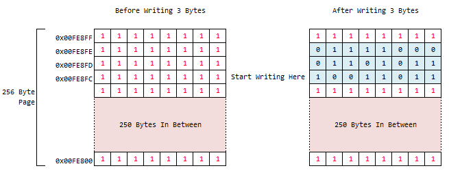
You have to send a valid address and at least a full 8 bits, otherwise the AT25SF081 will abandon the operation and nothing will be committed. If the memory is in a protected state (covered in overview part two), then the operation will be abandoned as well.
It takes a bit of time for the memory to be programmed, and you shouldn’t attempt to perform other operations on the chip until this completes. You can check the status of the programming state by querying the Status Register Ready/Busy Status bit, bit 0, in the first Status Register byte. The datasheet specifies a time of 5µs necessary to program a single byte, and .7ms (700µs) to 5ms (5000µs) to program an entire page. However the datasheet also says it is more efficient to simply poll the Status Register RDY/BSY bit, rather than trying to estimate the length of time of a program operation. The WEL bit is cleared at the end of the operation automatically.
AT25SF081 Erase Commands
Memory can be erased in blocks of 4K, 32K or 64K bytes, or the entire memory array as a whole can be erased. The block erase opcodes are 0x20 for a 4K block erase, 0x52 for a 32K block erase, and 0xD8 for a 64K block erase.
As with the Program operation, the WEL bit must be high before an erase operation can take place, and the memory must not be in a protected state. With the WEL bit set, CS low and the preferred erase opcode transferred, the address of the first byte to be erased in the block is transmitted. Even though you are erasing full blocks and not merely individual bytes, you have to transfer the full 24 bits of address data. It is important to be aware that regardless of what position within the block you specify, the entire block will be erased, both before and after that byte.
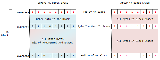
To erase the chip fully, you can use either of two opcodes, 0x60 or 0xC7. There is no difference in functionality between the two. Since you’re erasing the whole array, you don’t have to specify a starting address, just send the opcode and bring CS high.
In both cases, block erase or chip erase, you can poll the Status Register RDY/BSY bit to determine when the operation has completed, and the WEL bit will be cleared automatically. Times to perform the erase operations are as follows…
- 4K Erase: 60-300ms
- 32K Erase: 300-1300ms
- 64K Erase: 500-3000ms
- Chip Erase: 12-20sec
