In Part 6, we covered the how and the why of the Pin 13 LED, along with the related op-amp that appears there. We now leave the op-amps and power management behind and move into the Arduino USB connection that allows us to connect a computer to the Arduino to send and receive data. I would highly recommend grabbing a cup of coffee and a donut, because this is a longish post.
Build An Arduino UNO R3 from Scratch Table of Contents
A Confusing Arduino USB Connection Schematic
There are a lot of things on the left hand side of the schematic, and they all seem to be crammed together tightly, so that the drawing doesn’t flow off the left side of the page. Further, there are enigmatic symbols on there, like big black rectangles, that don’t really give you an immediate understanding of just what component was placed there, or what it’s purpose might be. As before, we’ll take this step by step and part by part.
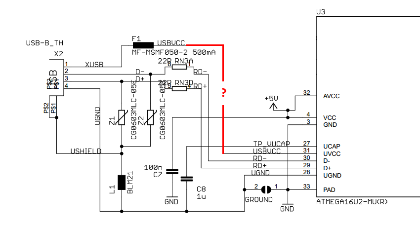
This is the official schematic covering the details of the Arduino USB connection. To try to clean it up a bit, I’ve blanked out all the portions that don’t directly involve the USB subsystem, but even after having done that, and enlarged the view slightly, part names and reference designators still sit on top of each other and make it a little daunting.
This circuit needs to do five things…
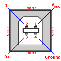
- Bring the USBVCC connection from the USB Type B jack, listed as VBUS in the USB documentation, to both the MOSFET in the voltage management section, and to the UVCC pin, USB Voltage pin 31, of the ATMEGA16U2 (henceforth referred to as the “16U2”) microcontroller.
- Connect the D- pin inside the USB jack to the D- pin of the 16U2, pin 30.
- Connect the D+ pin inside the USB jack to the D+ pin of the 16U2, pin 29.
- Connect the USB Ground pin inside the USB jack to the UGND pin of the 16U2, pin 28.
- Connect the USB jack shield, the metal housing that surrounds it, in a safe way so that doesn’t zap you, or zap the circuit.
USBVCC and the PTC
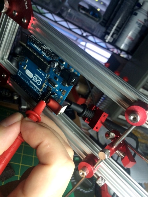
You can see I drew my own bright red line on the schematic with a question mark, because it’s unclear if there is a direct connection there, or if the USBVCC goes off to the MOSFET first, before connecting to the 16U2. Testing this is a little difficult, because to be absolutely sure, we need to use a multimeter to verify a path from the VBUS pin of the USB socket, which is only accessible under the board, to Pin 31 of the 16U2, located on the top of the board, and has a ridiculously small pin pitch. Fortunately, I have a PCBGrip System that is like a circuit testing tinker toy.
The upshot is that there is a direct connection from the VBUS connection in the USB socket to both the MOSFET Drain and the 16U2 UVCC pin.
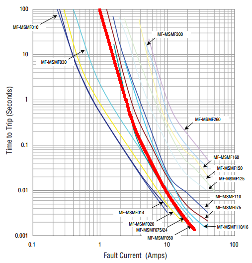
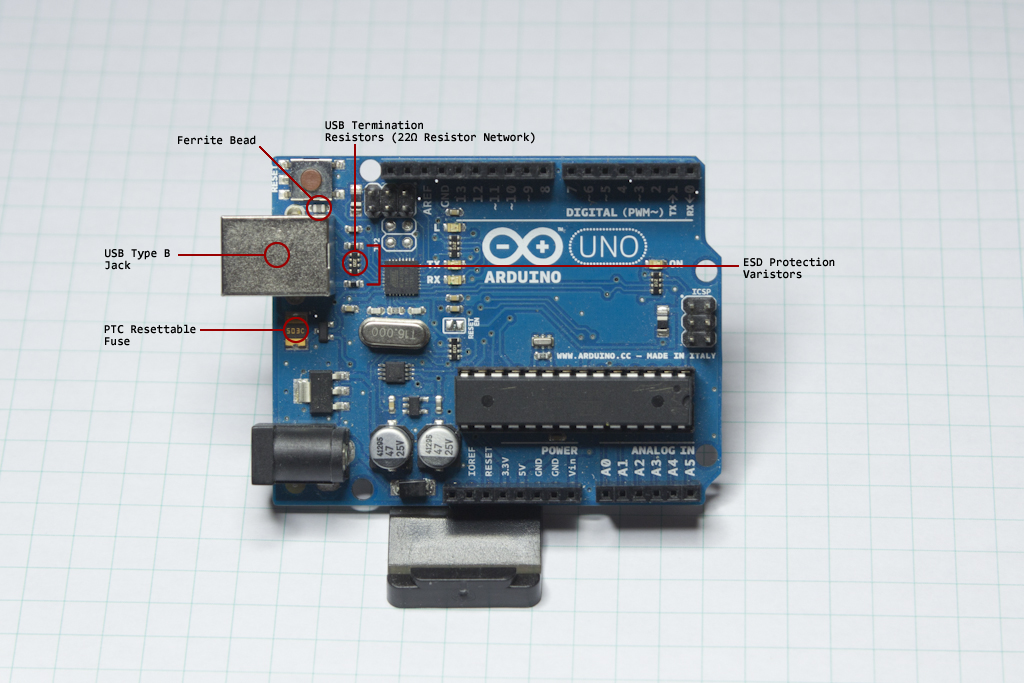
In series with this connection, and before USBVCC goes anywhere else, there is a black box on the schematic, reference designator F1. This is a Positive Temperature Coefficient (PTC) Resettable Fuse. This provides over-current protection from blowing up the USB host controller circuit in your computer. If you’re powering your Arduino from the USB cable, and attempt to draw too much current, say by short circuiting your +5V connection straight to ground (oh the many ways I’ve done this), the current spike causes a sharp increase in temperature within the PTC, causing it to immediately open the circuit. The circuit stays open until you deenergize the circuit and allow the PTC to cool off (takes less than a second). They list a Bourns part number of MF-MSMF050-2. This is a nice low cost, low risk part. According to the datasheet, it will hold a 500mA current load without tripping, then there is a grey area between 500mA and 1A where it would probably take a few minutes to heat up. Above 1A though, the “time to trip” drops rapidly, below 10mS for a 10A load. Now, if you’re connecting a constant current load to your Arduino for some reason, and slowly torturing it by dragging the load up from 500mA to 1A, then you’ll probably wind up damaging your USB host, yes. But that’s not the likely scenario. This is short circuit protection, where the resistance to current flow goes from “Some Value” to “Zero Resistance” in a heart beat, and the current goes from “Some Manageable Value” to “Theoretically Infinite” just as fast, meaning “Theoretically Instantaneous” protection.
D- and D+
USB signals are sent as differential pairs, mostly. Meaning a value is expressed as a difference between the level of D- vs. D+. There are certain instances where a single level is used, but for the zipping of serial bits back and forth between your computer and the 16U2, it’s D- vs. D+… that’s why there are two data lines.
The schematic shows a fairly direct connection from the USB jack to the 16U2, with three exceptions: a pair of serial resistors RN3A and RN3D, a pair of “things” tying each data line to ground Z1 and Z2, and the other “thing”, L1, that sits between the pair of things and the actual USB Ground rail.
The serial resistors, RN3A and RN3D, are acting as USB signal termination. This has to do with the concept of impedance matching between the cable doing the connecting, and the input on your microcontroller. As with nearly any topic that ever broaches the word “impedance”, it’s really, really involved. Let’s just break it down here into an analogy and then some Professor Farnsworth Patented Good News.
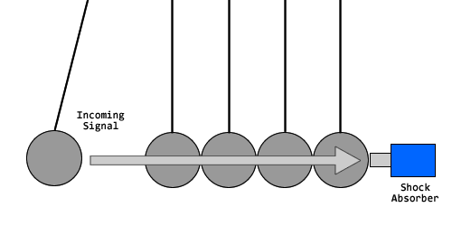
The USB signal travels down your cable from the host to your Arduino, pushing energy as it goes, like a whole bunch of inductors and capacitors in series, loading and charging really fast. Think of it like a Newton’s Cradle desktop toy, you send your signal by taking one of the balls and letting it swing down to hit the next one, and the signal propagates from one orb to the next down the line. When it gets to the end of the line, that last ball swings out, because there’s nothing there to stop it. Similarly (ok, in no way similarly but this is analogy-land), when your USB signal gets to the end of the transmission line, if there’s nothing there to stop it, it swings back and reflects up the cable to the host, like the last sphere swinging back at the end and reversing all the energy back to the original ball.
A termination resistor is like putting a shock absorber at the end of the cradle — it will take the full brunt of all that incoming signal, and dampen it so that the microcontroller gets the signal nice and cleanly, but nothing is reflected back up to the host.
The good news, everyone, is that the 16U2, as well as pretty much any device that acts as an upstream USB connection, tells you explicitly what size resistor to use! In the case of the 16U2, the datasheet says, “Serial resistors on USB Data lines must have 22 Ohms value (+/-5%).” Love it. Just tell me what to do, and I’ll do it. Boom, 22Ω +/- 5% 0805 resistor, Yageo RC0805JR-0722RL.
ESD Protection Varistors
As far as the two “things” go, they turn out to be Voltage Dependent Resistors, “varistors”. They act to provide electrostatic discharge (ESD) protection. If you’re all frizzed up with static electricity, because it seemed like a good idea at the time to wear wool socks while polishing a glass rod with a silk handkerchief on long pile carpet when it’s really dry before plugging in your Arduino, the sudden (and I mean sudden) voltage spike (and we’re talking kilovolts) causes the varistor to drop it’s resistance dramatically, giving a low resistance path to ground for the voltage, instead of letting it through your serial resistors (boom) and your microcontroller (expensive boom).
That USB Ground Rail, UGND has a lot of interconnections: the UGND pin of the 16U2, the big ground pad of the 16U2 TQFN package, the UGND pin from the USB Type B connector and the physical shield connections of the USB connection. So if the cable is carrying a static charge, or you have a static charge when you plug the cable in and your fingers touch the shield, you’ve provided a method for delivering that sudden overvoltage condition a path to follow: through the varistor, into the UGND PCB trace, back to the USB Ground pin of the Type B jack, through the cable and into Earth Ground of your PC.
The two varistors Z1 and Z2 are Bourns CG0603MLC-05E components. They’re designed to operate comfortably at 5V without affecting any operation, but as soon as there’s a spike above 20V, the clamping effect takes place to direct the pulse to ground, and above 100V the “minimum response time” is 1nS. The only problem I have with this component is that it’s an 0603, which is pretty small. I’ll mull it over later and think about supersizing it to an 0805 if I can find one.
You can well imagine that there are a TON of suggestions, guidelines and requirements to perform ESD protection on a circuit board. Have a look at this article from EETimes, that spells out a bunch of them. Some we’ll follow at layout time, some we won’t.
Ferrite Bead Filter
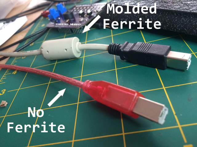
The final “thing” below the varistors, is a ferrite bead, L1. Ferrite beads resist high frequency noise, filtering them out of the signal media you’re using. Typically it would be used to eliminate any induced noise on the cable… for example, imagine you have an Arduino project in your kitchen, and for some reason you feel compelled to run your 10′ USB cable right over the top of your microwave. The cable would act as an antenna and pick up a bunch of junk noise from the microwave electronics. That high frequency noise would get dumped into the ferrite, where it is dissipated as heat. I don’t *think*, the ferrite has anything to do with the static discharge protection, but I invite anyone with far more experience in ESD or EMI protection to send me a note and explain it better. The ferrite on the PCB is similar to the big block ferrite that is molded onto the end of most computer cables. Most, but not all.
The part listed is a BLM21, which is more a class of components than it is a specific component itself. The key rating seems to be the current the device is able to tolerate, so we’ll just go with the nice low risk, 2A tolerant component in an 0805 package, the Murata BLM21PG221SN1D.
It is important to note that the connection from the USB shield to the UGND rail includes the ferrite bead, so we’ll want to make sure we follow the same path in the KiCad Schematic.
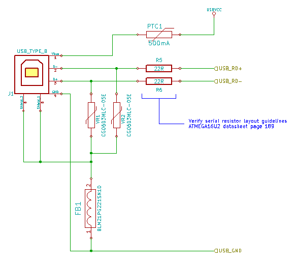
Arduino UNO R3 USB Connection KiCad Schematic and BOM
There are very loud and sanctimonious voices that can be found in various forums that complain against “just copying the schematic blindly without understanding it.” Well, I think we understand the basics of it, even if we probably couldn’t design it from scratch. My take away is: I have a device, this device has some sort of ESD and EMI protection, I have probably accidentally zapped this device at some point and it continues to work, therefore I’ll follow what currently exists.
You’ll see that the D+, D- and USB_GND connections just end it little signal flags, instead of going directly to the microcontroller. The way I’m designing the schematic is with hierarchical sheets, so at the master level, I’ll have interconnections between the subsystems, rather than trying to do it all on one sheet. Some people like trying to do it all at once so you can see the big picture, I like doing it by subsystems so the individual drawings are very easy to read.
Here is the USB Connection Subsystem BOM: Arduino Uno R3 From Scratch USB Connection Subsystem BOM
In part 8, we’ll work out the ATMEGA16U2 microcontroller subsystem.
