In Part 3, we defined the net names for our voltages in preparation for being able to keep them well sorted. This will now help us as we sort out how to keep the various ways of powering an Arduino from coming into conflict.
Build An Arduino UNO R3 from Scratch Table of Contents
The Dual Supply Problem
The Arduino allows you to connect a voltage source at the barrel jack, through the USB port and through the VIN shield pin header, and while it’s fairly obvious that the VIN pin and barrel jack shouldn’t be used simultaneously, there are many cases where you might need to keep the Arduino powered by a battery during a USB connect/disconnect.
Imagine you are doing some remote environmental monitoring with your Arduino Uno, and are storing the data in memory. You need to collect the data every so often, so you go to where the board is sitting and connect your laptop to it to download the latest figures. The act of connecting the USB doesn’t reset the board, so you know you can just plug in, open up the serial monitor window, grab your values, disconnect, and leave the Arduino sitting there, merrily monitoring away.
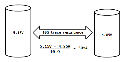
When you connect the USB cable, you instantly provide a 5V source that you know is able to power the Arduino when it’s just sitting on your desk. However, you also have a battery pack connected to it that is creating a nicely regulated 5V through the methods covered in Part 2. Since the 5V Fixed LDO Regulator and the USB 5V supply would both be trying to supply voltage and current at the same time, to the same things, that means they’d essentially be connected to each other. Neither of those are ideal voltage sources, meaning that neither is EXACTLY 5.00000V, they all have tolerance ranges and output will vary based on environmental conditions like temperature – TL/DR: their voltage level won’t be equal. What happens when you connect two voltage sources of different levels in parallel? You get a current loop flowing from the high voltage source to the low voltage source, and that’s bad, particularly if that current flow is going back up your USB cable into your laptop.
We don’t want that to happen.
Ridiculously Short Explanation of Op-amps
The solution is to automatically cut the 5V line coming from the USB (just the 5V supply, not the USB serial communication), the moment any voltage is detected on VIN high enough to kick on the 5V Fixed LDO. It would be great if we could just write some code that says, “if (VIN >= 7V) then turnOff(USB_5V);“. Well, I’ll do you one better… how about implementing that “if” statement in hardware. To do that we need to use an Operational Amplifier (op-amp).
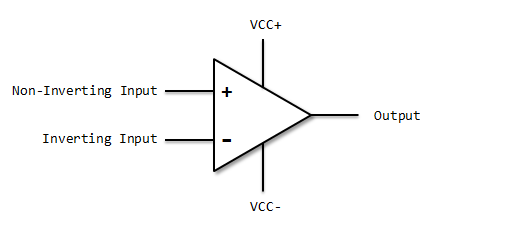
The definition of an op-amp I’m going to give you is equivalent to saying “The Saturn V was a mechanical device that took people from Point A to Point B”. Be that as it may: an op-amp is an integrated circuit that accepts two inputs, the “non-inverting” and the “inverting” inputs, and attempts to balance any difference — even very small differences — between the two by driving the output as close to the op-amp’s supply voltages as it can, VCC+ and VCC-. This simple transaction can be harnessed to accomplish millions of different tasks. You can take the output and feed it back to one of the inputs, you can add resistors and capacitors in there to create amplification. But we don’t care about any of that… all we care about is: if there’s a difference between the non-inverting and inverting inputs, it will try to balance it by driving the output to VCC+ or VCC-, and doing it awfully fast.
VCC+ and VCC- are connected in one of two ways. “Dual Supply” means that VCC+ is something like +9V and VCC- is -9V. Think of an A/C sine wave constantly going up and down about a 0V x-axis, like an audio signal… gotta have some value above 0V and some value below 0V to be able to cope with that signal. “Single Supply” is the case where VCC+ is some positive voltage, in our case +5V, and VCC- is some lesser value, typically (and in our case) ground. This sort of supply is great for comparators, where the inputs won’t ever go below 0V. When an op-amp is described as “rail-to-rail”, that means the output can be driven awfully close to the VCC+ and VCC- values, as opposed to sort of loosely getting close to those values.
That means there are three states we need to concern ourselves with: inverting higher than non-inverting, inverting lower than non-inverting, inverting and non-inverting exactly equal.
Non-Inverting > Inverting = Output Driven to VCC+
Non-Inverting < Inverting = Output Driven to VCC-
Non-Inverting = Inverting = No Output
Hopefully you are starting to see the if statement taking form in hardware.
Voltage Conflict Management: The Op-amp as Comparator
Let’s list what we know about our circuit before we dig into how we’re going to deal with it.
Voltages
- We have +5V coming from our USB cable. Call this USBVCC.
- We have +5V coming from our 5V Fixed LDO. Call this 5V_LDO.
- We have some higher voltage coming from the barrel jack or the shield pin header. Call this VIN.
- We have +3.3V coming from a 3V3 Fixed LDO (you’ll see in a second). Call this 3V3_LDO.
Desired Outcomes
- When USBVCC is connected, and VIN is not connected, we want to allow USBVCC to supply 5V.
- When USBVCC is not connected and VIN is connected, we want to allow VIN to generate 5V_LDO to supply 5V.
- When USBVCC is connected, and VIN is connected, we want to cut off USBVCC and allow VIN to generate 5V_LDO to supply 5V.
There it is. Using the four different voltages and some hardware, we want to be able to create the three outcomes. We do this by using an op-amp as a comparator. We’ll test the voltage level of the VIN rail, and if it’s below some reference voltage, we’ll allow the USBVCC rail to supply voltage. If it’s above some reference voltage, we’ll prevent the USBVCC rail from supplying voltage.
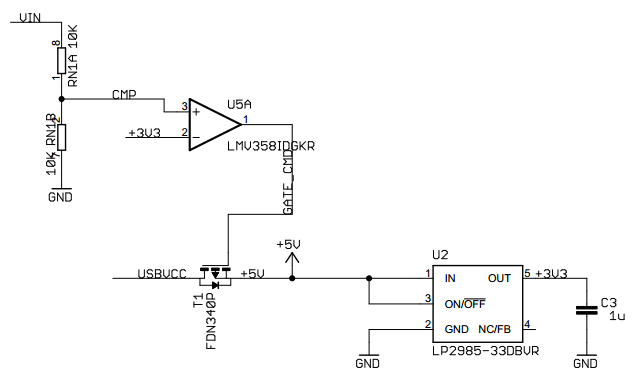
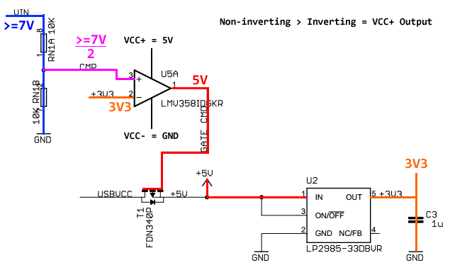
Here is the comparator circuit from the official schematic…
Let’s examine the schematic against what we want our outcomes to be.
USBVCC = Connected, VIN = Disconnected
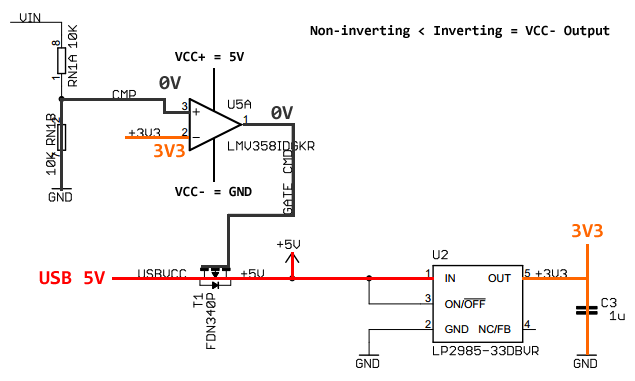
When VIN is disconnected, the CMP net entering the non-inverting input of the op-amp, U5, is at GND (tied through the 10K resistor, RN1B, to GND), and the inverting input of U5 is held at a reference voltage of +3.3V. Because the non-inverting input is lower than the inverting input, the output is driven to VCC-, in this case GND. The output is connected to the gate of the P-channel MOSFET, T1, and since it’s at GND, that means the MOSFET will allow electrons to flow like a closed switch. USBVCC is then connected to the +5V net, and also powers U2, which is a 3.3V Fixed LDO Regulator. The output of that LDO supplies the 3V3 voltage to the shield pin header, but also is used as the voltage reference for the comparator.
USBVCC = Disconnected, VIN = Connected
When VIN is connected, it energizes the voltage divider at the non-inverting input of U5. The op-amp will compare this against the 3V3 reference on the inverting input. The voltage divider is comprised of a pair of 10K resistors, so you’ll see exactly half the VIN voltage at the non-inverting input. In order for anything to happen that’s different than our previous state, we would need at least 6.61V (6.61V / 2 = 3.305V). Realistically, because of the drop out voltage, this voltage will be at least 7V (divided by two) and more likely 9V (divided by two). Regardless, as soon as you cross that threshold, the op-amp will flip to the opposite state and will send VCC+ to the output. With 5V at the output, that means 5V at the gate of the P-channel MOSFET and it flips the MOSFET into an OFF state, cutting USBVCC out. Since in this case, USBVCC isn’t connected, it doesn’t really matter. 5V is still supplied to the 3V3 Fixed LDO from the +5V rail (from the 5V Fixed LDO), which preserves the reference voltage of the comparator.
USBVCC = Connected, VIN = Connected
There is no essential difference between this state and the state above. Since VIN is energized, and VIN is a voltage above 7V in the real world, USBVCC is cut off from the 5V rail by the same logic.
In Part 5, we’ll select components to match the functionality shown on the schematic.
