I thought it might be helpful to take an electrical view of the shift register pins when you’re pressing the buttons, so that you have some basis for comparison when you see the equivalent actions being performed by code. If you have an oscilloscope you can follow along. If you don’t that’s perfectly ok. There are full color screen captures below to use as well.
Objectives
- To visualize the input signals that make a shift register work
- To visualize the movement of data inside the shift register
Background
Fundamentals of Serial Communications
Schematic
Education Shield – Shift Register Subsystem
Setup
For this module, you’ll need the following equipment:
- Education Shield or the Manual Serial Communications Trainer
- Arduino UNO R3
- Oscilloscope with at least two available channels
1. Mate the Education Shield with your Arduino UNO R3, and connect the UNO to your USB.
2. Upload code to your Arduino setting the pin mode for pins 6, 7, and 8 to INPUT. This ensures the pins are in a high impedance state, and won’t interfere with your measurements. You can add the following three lines of code to the setup section of the “Bare Minimum” sketch easily.
|
1 2 3 4 5 |
void setup() { pinMode(6, INPUT); pinMode(7, INPUT); pinMode(8, INPUT); } |
3. Connect your oscilloscope probes to the CLOCK, DATA, LATCH. You can do this by placing jumper wires into the female headers for pins 6, 7, and 8, and using the hook connector of your probe on the other end of the jumper. If you only have two channels on your scope, measure CLOCK and DATA. Ground reference for your scope can be obtained from any of the ground sockets on the Education Shield.
Alternatively, you can use the Manual Serial Communications Trainer instead. Connect 5V and CLR to 5V, GND and OE to GND, DATA to D8, LATCH to D7, and CLOCK to D6, and run the code snippet above.
Manual Clock Examples
In The Beginning
Our shift register begins with all eight outputs, QA through QH putting out 5V, to light our LEDs. The “Q” designation meaning the “SET” output vs. “RESET”. See the post on Flip Flops to refresh your memory on this. They are labeled A through H because some engineer at Texas Instruments woke up that morning and decided they would be listed in sequence alphabetically instead of numerically. This means that we have a logical 1 in each of those positions.
![]()
Example One: Turning off the first LED
In the Fundamentals module, the first example had you turn off one of the LEDs by pressing the CLOCK button, then pressing LATCH. What you see in this display, are three traces labeled “CLK” in Yellow showing the CLOCK button, “DATA” in Purple showing the DATA button and “RCLK” in Blue, showing the LATCH button (“Register Clock”, you can only use four characters to label a signal an RCLK is the official TI designation). I’ve arranged the three traces so that CLK is at the top, and DATA is immediately below. If DATA goes high, it will overlay across the CLK signal so it is easy to see if the timing is correct. RCLK is moved down so that it’s very obvious when it is pressed, isolated from everything else. The horizontal scale is a half a second per division (so the whole screen represents six seconds of time) and the vertical scale is 5 volts per division, so when a signal changes its logic state, you should see it move the equivalent of one division.
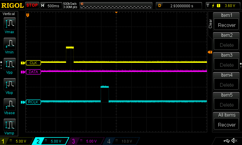
In this first example, the CLK line went high, but DATA was low and then that zero was latched into the storage register. The clock signal was high for around a quarter of a second (eyeballing it), and the latch was high for about the same length of time. That time period, 250ms, is the length of time my finger had the button down.

Inside the shift register, you started with all 1s, then a 0 was shifted into the MSB position, forcing the 1 in the LSB position out.
Example Two: Turning off two more LEDs
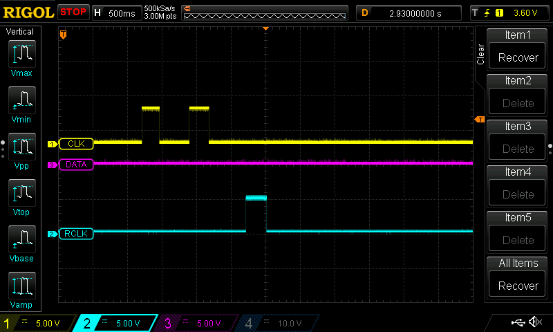
There are are an additional two pulses on the CLK, and DATA remained low, consequently, two more zeros were clocked in. The internals of the shift register reflect this, showing two ones being shifted out as the two zeros are shifted in. RCLK goes high to latch in the value.

Example Three: Turning off the remaining LEDs
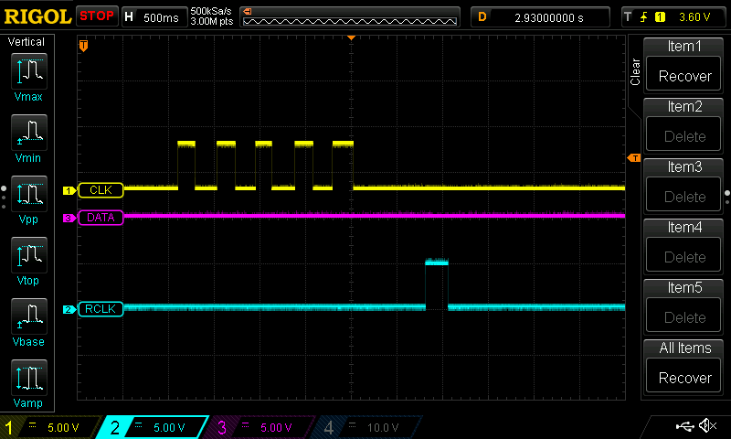
Finally, the remaining ones are shifted out as five more zeros are clocked into the register.

Example Four: Turning one LED back on
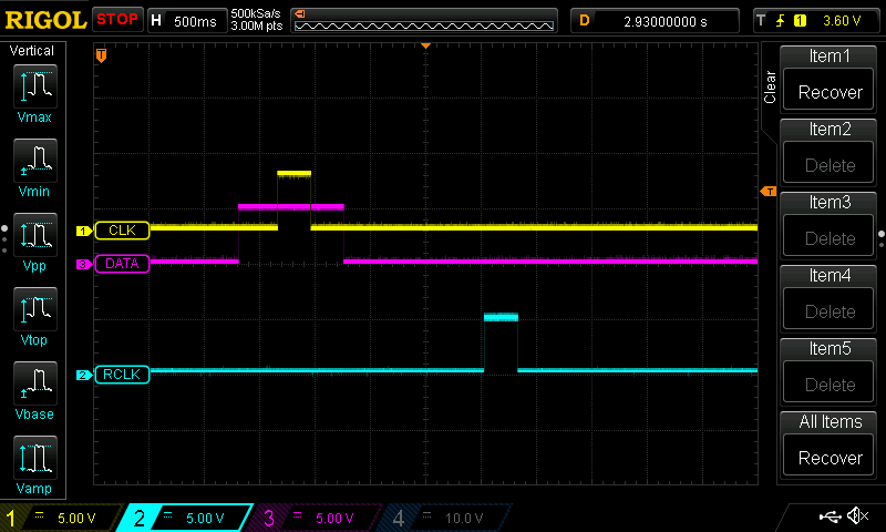
Now it gets a bit tricky as we need to coordinate our fingers, and press two buttons in the correct sequence to start clocking in ones instead of zeros. You can see that I raised the data line high for nearly a full half second before I cycled the CLOCK button, ensuring that the data signal would be in a high state on the rising edge of the clock signal.

Example Five: Turning the remaining LEDs back on
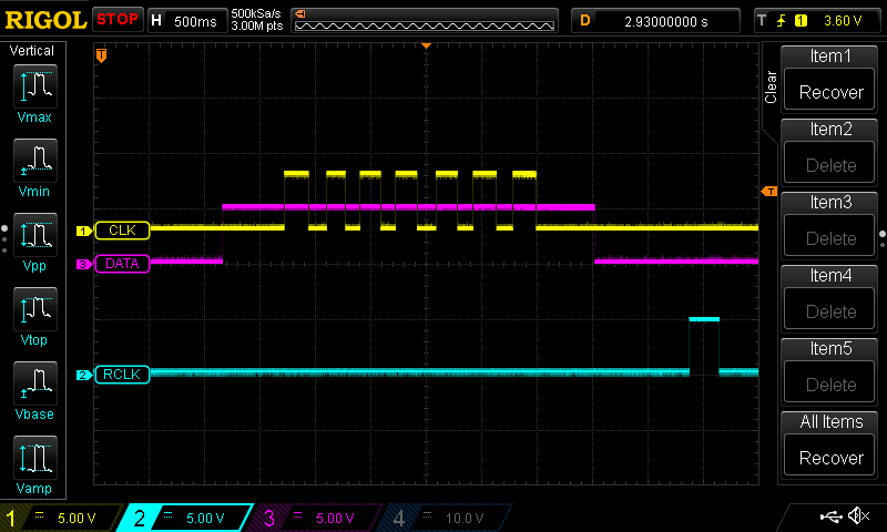
I merely held the DATA button down while I hammered away at the CLOCK button seven times. An alternative method would have been to raise and lower the data signal for each clock sequence, however as you’ll see when we move into letting our microcontroller handle this, if successive bits are the same as the last bit, the data line is kept in the same state conveniently.
The end result being that we return our shift register to the state it was in originally.

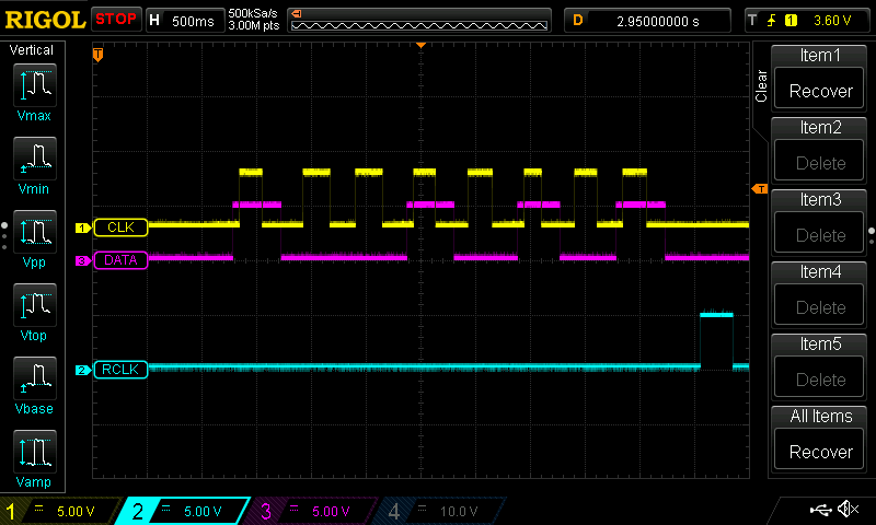
Here are the remaining examples, showing the full bytes being entered into the shift register. Remember that you’re reading the oscilloscope left to right, so the first button press I perform is at the left and the last button press I did is on the right (always the RCLK button press), so you should be able to tell if I was entering the most significant bit or the least significant bit first.
Example Six: Full Byte B10101010
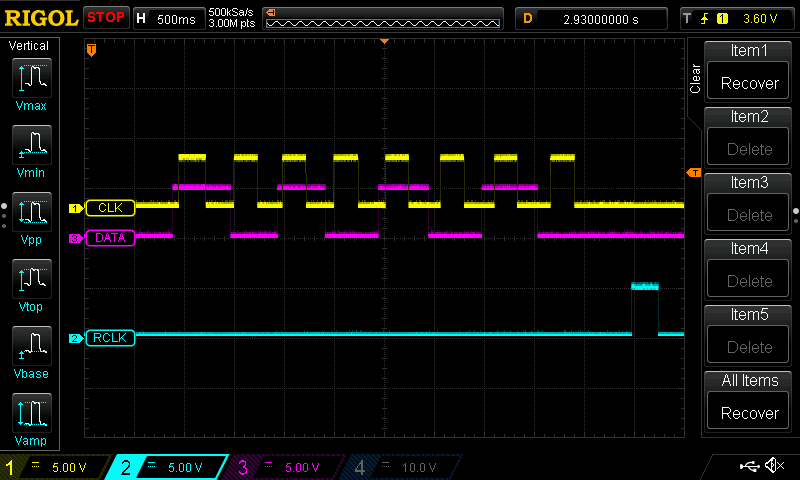
Example Seven: Full Byte B00011000
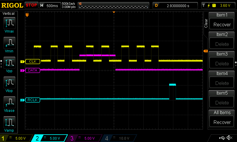
Example Eight: Full Byte B10010101
