This module begins our discussion of I2C basics by introducing the theory, structure and signalling of the I2C serial communications bus. This is just an overview, with the most important aspects receiving their own dedicated modules to provide greater detail.
Objectives
- Understand what I2C stands for.
- Understand how components on the I2C bus are connected.
- Understand why pull up resistors are essential.
- Understand what an I2C address is and when variable addresses are used.
- Understand what the I2C General Call address is.
- Understand the various signalling conditions.
Background
This is the first module describing I2C, consequently, reading through the previous sections will be helpful for the less experienced, but are not necessarily essential. Here are some additional resources for those interested in obtaining greater technical detail…
- Wikipedia Article on I2C
- PDF of the Official NXP I2C User Manual
- PDF of the NXP I2C Application Note
Schematic
No schematic is associated with this module.
Setup
This module is dedicated to I2C theory, so no hardware is necessary at this point.
I2C Basics: Origins
I2C (or as one of this project’s original Kickstarter backers requested it be referred to, I²C), is a communications bus used to get chips to talk to other chips. The standard was originally defined by Philips (now NXP after being spun off in 2006) in the 1980s, to help reduce the component count (and lower component counts mean lower costs) in their retail television designs. Consequently a lot of their documentation repeatedly refers to consumer electronics in general and TVs in particular. The Atmega microcontroller at the heart of your Arduino has two pins that have internal guts dedicated to this system, and are able to interface with any other chip that is built to the standard. Chips are talking to chips – Inter Integrated Circuit – IIC – I2C (or, yes, I²C). TWI or “Two Wire Interface” is a subset of the I2C standard implemented by other manufacturers and is the reason why the library supplied with the Arduino IDE that we will eventually use to talk with these chips is called the “Wire Library”.
I2C proved so popular, that it grew into the vast array of signal processing and sensor technologies you have available today, and the specification has grown to allow greater speeds and larger quantities of I2C compatible components to be used in a design.
Typical speeds on an I2C bus are 100kHz “Standard Mode” and 400kHz “Fast Mode” for the purposes of Arduino users. Additional speeds exist from 1000kHz “Fast Mode Plus” up to 5Mhz “Ultra Fast Mode Plus”. All speeds use 8 bit byte data frames.
I2C Basics: Hardware Details
SDA and SCL
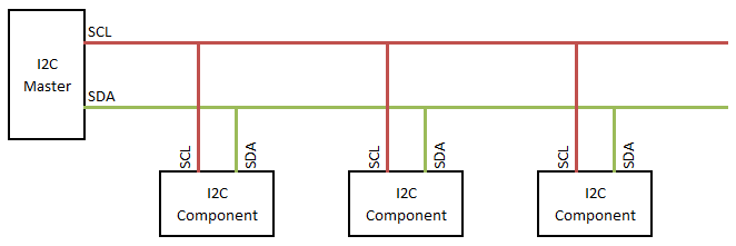
The I2C specification lays out two buses for communication: the Serial Clock bus or SCL and the Serial Data bus or SDA. The term “bus” used to mean, specifically, wires in parallel connecting nodes, but now just generally means “a bunch of stuff all hooked together in common”.
Amount Of Devices
The amount of devices that can be connected to an I2C bus is directly related to the capacitive loading of the design being considered. The official NXP I2C manual (page 11) states that this capacitive loading is limited to a maximum of 400pF. What is meant by “capacitive loading” is a pretty involved topic, but generally, each of the SCL and SDA pins in your system will have some form of native capacitance inherent in their design, and the actual copper trace on your PCB will too. The pin capacitance is fixed by the chip manufacturer but the PCB trace will increase in capacitance as it increases in length, which is one of the reasons why I2C is considered to be a short-run technology. As the capacitance of the bus increases, it makes it more difficult for the system to snap a signal to a logic high or low, thus the 400pF limit.
Pull Up Resistors
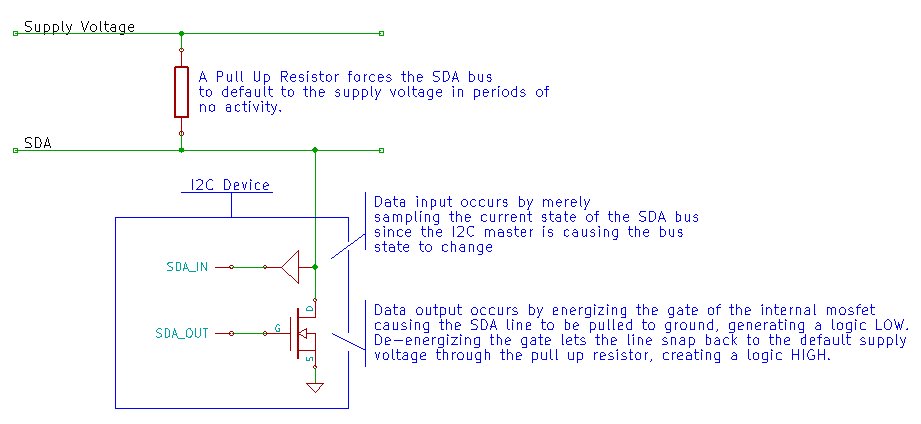
I2C pins are designed as “open drain”. This means that they are unable to actually drive any current at all, they can only sink it… dispose of it… send it down the drain. That means the designer has to provide the voltage and current source, and that signal has to be available at all times in order to generate a logic high. That is accomplished using pull up resistors on the SCL and the SDA buses, which is a common item to note on any I2C related schematic.
Addressing
There is no addressing bus in the I2C standard, or “chip select”, so all determination of who needs to be paying attention at any particular time is determined through software, using 7 bit addresses that are hard coded into the devices being used (10-bit addresses are used on higher signal speed components beyond the ability of an Arduino). Even though the original patents for I2C have expired, an organization called the I2C-bus Committee still maintains the official repository of I2C addresses and controls which manufacturers are allotted which addresses. For those familiar with IT work, I2C addresses could be thought of as MAC addresses for NIC cards.
Some manufacturers provide ways of selecting between an array of addresses by tying address pins of a device to Vdd or GND. This is done when a single device type can appear many times on a bus. For example, an industrial system may need to measure temperature at many different points in an enclosure, so having five or six temperature sensors on the same I2C bus would make sense. Consequently, each of those sensors would need to have unique I2C addresses; if you weren’t able to modify the address, you would only be able to have one of those sensors in your design.
From the datasheet for the Atmel AT30TS750 Temperature Sensor that is on the Education Shield…
The A2-0 pins are used to select the device address and correspond to the three least-significant bits (LSBs) of the I2C/SMBus 7-bit slave address. These pins can be directly connected in any combination to VCC or GND, and by utilizing the A2-0 pins, up to eight devices may be addressed on a single bus. The A2-0 pins are internally pulled to GND and may be left floating. However, it is highly recommended that the A2-0 pins always be directly connected to VCC or GND to ensure a known address state.
General Call Address
Instead of transmitting the 7 bit address to interact with a specific component, the I2C master may issue a general call address of 0x00. Any device that is capable of receiving data will respond with an ACK. This is typically used for resetting the I2C bus.
I2C Basics: Signaling Details
I2C signals travel on the SDA and SCL buses and have developed over time to allow several different communication speeds. The Arduino is able to communicate with the first two: 100kHz Standard Mode and 400kHz Fast Mode. Ultra Fast Mode and others are beyond the scope of what you can accomplish with your Uno.
The I2C default state, the calm state during which nothing is happening, is called the Free State, and is noted as having both the SCL and SDA lines at logic high. This makes sense as they are in that state by default due to the pull up resistors. The act of establishing communications and sending data back and forth follows a very formal structure.
Communication starts when the master pulls the SDA line low while the SCL line is high. This is called the Start Condition. When the start condition has been established, the bus is no longer in a free state, but is considered in a busy state. The start condition is the signal to the slave components down the line that they need to start listening.
After the start condition has been established, the master immediately transmits the address on the SDA line sending the seven bits of the address followed by a READ / WRITE bit that will indicate if the master is planning on reading from the addressed component or writing to it, WRITE is active low, so READ would have the SDA line high on the 8th bit — WRITE would have the SDA line low on the 8th bit.
With the start condition created, the address transmitted and the R/W bit sent, the slave now has to send an acknowledgement or a non-acknowledgement, called an ACK/NACK. Immediately after the master has sent the R/W bit, it releases control of the SDA line, and listens on the next clock pulse for the slave to pull the SDA line low: a low SDA on the ninth bit indicates an ACK from the slave. Again, this makes sense: any I2C device must be an active participant in creating logic low states, so using a low SDA signal means that the slave component is not busy performing some other task and is ready to perform communications.
If the ACK was detected by the master, data is now sent/received 8 bits at a time (one byte). After each byte, an ACK has to be sent by the slave to allow the master to know that everything’s still happening as it should. Communication then flows in this manner — 8 bits + ACK — until the full set of data has been sent. After the final byte has been sent, either the master responds with a NACK indicating that it has received everything, or the slave does if it is receiving, and then the master initiates a stop condition… SDA transitioning from low to high while the SCL bus is stable at logic high.
If in the sequence of communication an ACK is missed, or an NACK transmitted, the master will immediately set a stop condition and return the SCL and SDA buses to the logic high state.
Next Up…
Next we’ll cover the hardware and signalling specifications in greater detail.
