August 4, 2014
I had Digi-Key ship the parts to the UPS depot down the street, and they arrived, last Friday, but no one told me. I was also not told that there would be a +$10 storage fee at UPS Store. It’s almost like they really don’t want my business.
Quick check showed that the parts will fit, but will they work? WILL IT BLEND?!?
August 11, 2014
Transcribed the build log notes from Notepad++ into the website. Didn’t realize how much I’d actually kept track of until now!
I should probably start trying to build the thing at some point too.
* * *
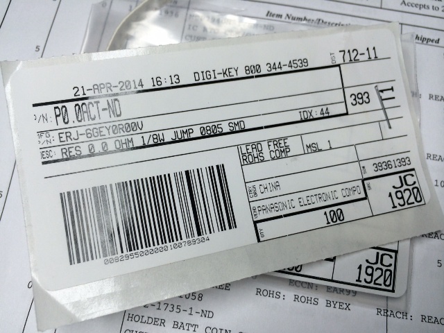
Decided to start with the shift register circuit, since all the resistors and LEDs are middle of the top side copper and would be difficult to get to when other things get soldered down. However, just as I finished sorting out all the parts, I realized I didn’t order a single 0Ω resistor. I think I’ve got quite a few left over from the BenchBuddEE build, so I’m not dead in the water, and I could bodge wires across or bridge with solder if necessary… but this, this is how it starts. Brilliant.
A mystery of the universe: how to tell the anode from the cathode on a SMD LED without an electron microscope.
* * *
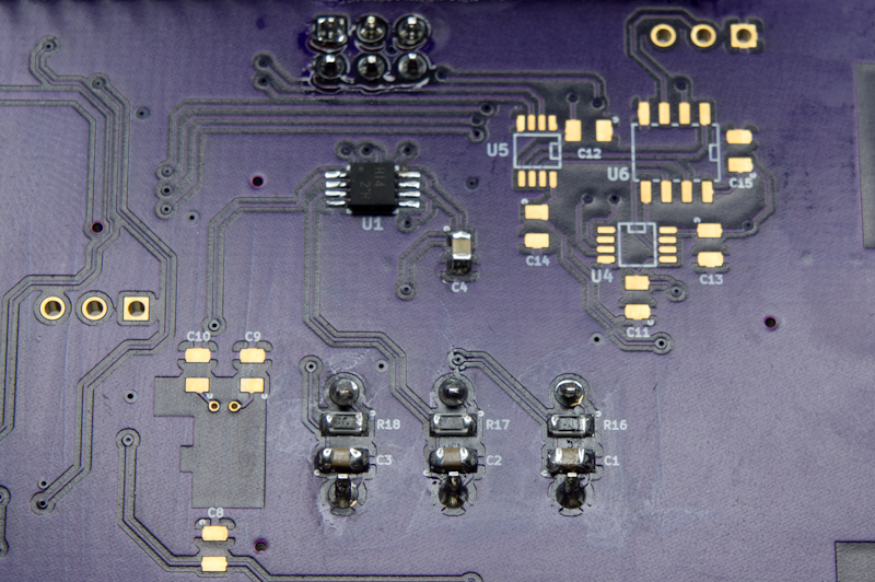
Shift Register circuit and the debounced switches are soldered down and working! Not a bad start! My fears of having to hand solder a SSOP component, the backside mounted Schmitt-Trigger Inverter, were apparently unfounded. That thing went on remarkably easily.
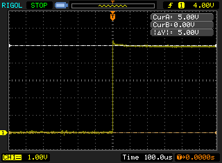
I suspect it was my experience with building the shift register out on the breadboard, without debounced buttons, that made me leery that this would actually work as I hoped, but I guess that’s what correct engineering does 🙂 The clock button only submits one clock signal per press, which is exactly as it is supposed to work.
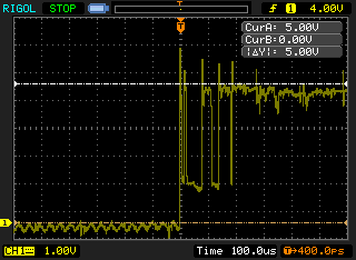
For comparison purposes here is an undebounced clock signal input…
…and a debounced clock signal input…
August 12, 2014
With a mind to assembling the board module by module, I’m going for the RTC right now. Turns out the spacing between the crystal and the temp sensor would make it pretty difficult to get the soldering iron in to solder down the IC, so I’ll put that in place first. Not my favorite thing to do, because that just makes troubleshooting I2C trickier if it doesn’t immediately work.
* * *
Well putting down the temp sensor before the crystal was a good idea. If only I’d done it both times. Got distracted between boards and put the crystal down before the AT30TS750 on the second board. Guess it wasn’t all THAT much more difficult, but still, the thought process made sense.
* * *
Hooked it up and sent some code to get back the first seven bytes from the RTC, and got back -1 as the response on all bytes. Hmmm. OH! look, I didn’t put down 0Ω resistors for SDA/SCL. Oops.
Now they’re down and… still getting -1 back on all bytes. Tricky. Also, I forgot to put test points on the boards, so I had to bodge a jumper to the ground pin to make oscilloscope use easier… and trimmed off LED leads onto the SCL/SDA pins. Unto the lands of troubleshooting I go…
* * *
So, five hours later… turns out, you have to turn the clock on. And does one turn the clock on by applying power to Vcc? No. Does one turn the clock on by flipping the “TURN THE CLOCK ON” bit in, say, the control register? No. Perhaps it might be in the entire register dedicated to, you know, the oscillator? No. Ahhh… of course! IT’S IN THE SECONDS REGISTER! And it’s not called “TURN THE CLOCK ON”, it’s called “Start Oscillator bit: 1 = Enabled / 0 = Disabled”, abbreviated ST. Such clarity! So intuitive!
Good thing I didn’t do anything drastic like chop the crystal off thinking I’d destroyed it, or solder on a different crystal with different load capacitance, or stare at the datasheet defying it to continue to be impenetrable.
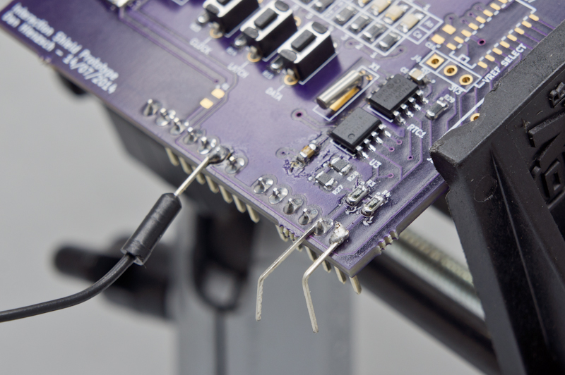
It works now on both boards. Now that I am getting responses, I can actually look at the data registers and… wow. Microchip really liked sticking configuration bits all over the place. Lots of masking has to be performed on the data returned. Well, regardless, it’s working, I’ll worry about figuring that stuff out later.
Altered the test code a little and the AT30TS750 temperature sensor came up immediately and provided accurate data. I should consider moving the chip elsewhere on the board, because it appears the ATMEGA328 is heating the Education Shield, and the temp sensor is sitting squarely above the ATMEGA. Add it to the list.
August 13, 2014
Before I move onto the SPI circuits, I wanted to check the battery backup feature of the MCP7940. You have to flip a bit in the RTCWKDAY register, so after doing that, it worked flawlessly. Since all of the registers on this thing have definite purpose, and there are a buttload of them, writing a library to make it more functional will probably be a necessity. I’ll need to figure out how to do that, without abstracting too much… the idea is for people to get their hands dirty playing in the bits.
Also, the difference between the original example schematic published by Microchip in the MCP7940 datasheet, versus the one published in the “DS1307 to MCP7940N Migration” AppNote with regard to the backup battery is pretty significant. I’ll need to revise the production board.
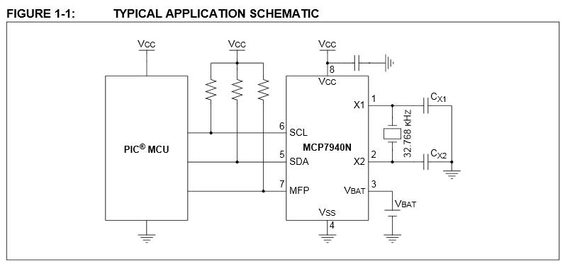
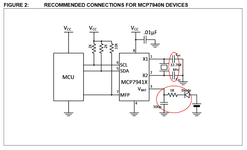
Having the LED’s with the shift register is a convenient way to display full bytes and visualize the affects of bitwise operations. I need to incorporate that into the learning.
The pads of the SOIC16 footprint direct out of KiCAD don’t leave any copper exposed past the tips of the pins – makes it hard to ensure good connections visually. I’ll need to modify those for ease of production I think.
ADC circuit is soldered down. Added some more bodge wire test points to MOSI / MISO / CLK and CS_ADC. Conductivity test was good: AGND is live, 3V3 is live, MOSI / MISO / CLK are connected and correct, and CS_ADC is good too. That was a lot of 0Ω resistors for one chip! Time to code.
* * *
Important things to note from a datasheet when looking for SPI characteristics…
- SPI Mode: The ADC works with both 0 or 1
- Clock speed: The MCP3008 expects clock high times of 125nS, which means 4Mhz / 4.
- Address Method: How do you tell the chip which register you want to talk to?
- MSB vs. LSB: In this case, MSB.
The good news is, the ADC is working exactly as it’s supposed to. The bad news is that I’m struggling with telling it how to send me the second byte of data. I know the solution is obvious, but I just haven’t remembered what it is yet.
* * *
Ok… the problem was my thinking, and I’m ok with that. The ADC uses three bytes and I’m used to doing it one byte at a time asynchronously. Send address … Request Byte 1 … Request Byte 2. Well, in this case, that first byte is almost entirely empty… seven leading zeros followed by a command bit and then three address bits for the 8 different channels of the ADC (0-7). So my thinking was, send the two address bytes out, then ask for the two bytes of data back. That’s four bytes though, meaning you’re getting junk signal back.
Here is the how I did it at first, which was wrong…
|
1 2 3 4 |
SPI.transfer(B00000001) // send that 1st command bit with the seven leading zeros - ignore any returned data SPI.transfer(B11100000) // send that 2nd command bit, specifying ADC Ch7, and then zeros - ignore any returned data ch7MSB = SPI.transfer(junkData) & 0x03 // get back the 1st byte of the 10 bits of data, keep only the two LSB. ch7LSB = SPI.transfer(junkData) // get back the 2nd byte of the 10 bits of data, keep it all. |
The problem there is that the MSB byte is actually the LSB byte… and the LSB byte is… who knows… ether… crap… crackle of the universe… no idea. But you can see how I was trying to do it one step at a time. WRITE … WRITE … READ … READ. Well, here’s the timing diagram:

When you’re sending out the “Request data from the ADC channel 7” command, at the end of that byte, you’re already getting valid data back – the last two clock cycles of that second byte. God, typing that out it seems so simple now!!! Here’s what I was seeing, though, when that code was ran…
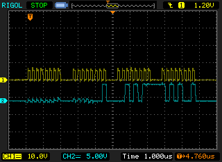
CH2 is the MISO line, and you can see that with the code above, I’m loading that fourth mystery byte into ch7 LSB, even though the timing diagram doesn’t show a fourth byte – consequently junk data. The solution is sooooo simple! You can read AND write in the same command!
|
1 2 3 |
SPI.transfer(B00000001) // send that first command bit with the seven leading zeros ch7MSB = SPI.transfer(B11100000) & 0x03 // send the ADC Ch7 address AND record the returned data, keep only the two LSB. ch7LSB = SPI.transfer(junkData) // get back the 2nd byte of the 10 bits of data, keep it all. |
Here’s the result of that bit of code…
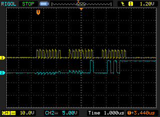
Three bytes only, and I’m loading that second byte in right away. I guess I’d never wrapped my head around the fact that you can send data out on MOSI and receive data on MISO in the same byte! That’s what I get for playing in I2C first.
August 14, 2014
Time to play with the AT25F512B Flash chip! I ran across this excellent Instructable by user ptorelli, about building an Anemometer using a Winbond IC, which was the one that went end of life as I was building this BOM. I chose the AT25F12B because I believe it will be a near drop in replacement. His code is remarkably easy to comprehend, so I intend to usurp much of it with enormous gratitude to the original author.
Well, the Pin 1 marking on the Adesto chip is nice and obscure. I think it’s a little triangle between pins 1 and 2. I think. Guess we’ll find out.
* * *
Flash circuit is down on both boards, soldering the level shifters with their LSSOP footprints was a brass plated pain in the ass. I should try again to find something in the SOIC range that doesn’t cost a fortune instead. I think I used a pair of them to make routing the lines easier.
Went through tested conductivity between all the pins to make sure there were no solder bridges, and then each segment end-to-end, ie: ARD-MOSI to LEVEL SHIFTER to AT25F512B MOSI and everything toned out fine, to use an old telephony term.
SPI Characteristics of the AT25F512B…
- SPI Mode: The Flash IC works with 0, 1, 2 or 3.
- Clock speed: The Flash IC is capable of up to 104MHz speeds, well faster than the Arduino.
- Address Method: Opcode clocked out first, followed by register then data.
- MSB vs. LSB: In this case, MSB.
Well, first attempt at running the thing and I get bupkus back on MISO. And since everything is on the bottom side copper, including the level shifters, and is sandwiched squarely against the Arduino – and as mentioned before I don’t have any test points – this will be exceptionally difficult to troubleshoot. If I’d put real shield headers on these things, this would be a lot easier.
So… bodged a wire onto the Flash IC MISO pin to extend it out from under the board and see if it was being shifted 5V to 3V3… then remembered that I didn’t put that through the level shifter. Puzzled and puzzled til my puzzler was numb, then decided to bodge the wire onto MOSI instead. Brought it up… certainly shifted from 5V to 3V3… also looked exactly like the clock signal…

Oops.
Now to figure out how to fix this…
- Cut the traces near the level shifter, scrape away the solder mask and cross wire the signals to their correct position. This is difficult since the traces are 10mil tiny, and the vias have no exposed copper.
- Lift the 0Ω resistors from SCLK and MOSI, and bodge a pair of wires to correct the problem. This means that the board would only function for the Flash IC, and the problem would be brought over to the ADC then.
- Bodge wires around to the back of the board from the 0Ω resistors and solder them directly to the level shifter, then cut the traces in an easy spot on the top side copper. This would allow the board to work for both SPI modules.
* * *
Well, it’s a resoundingly hideous hack, but it works. Went with option three and for once was grateful I had these spindly throughhole resistors from RadioShack. Their leads were teeny enough to solder onto the pins of that LSSOP footprint without shorting the pins together with their girth. It’s fraaaaagile though – can’t imagine it will sustain too much in the way of handling, so each time I seat it on or remove it from the Arduino, I’m hastening it’s demise. But for now, it’s definitely working!
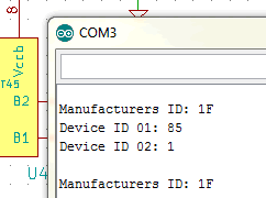
So, that’s each module communicating correctly. Now what to do… what to do…
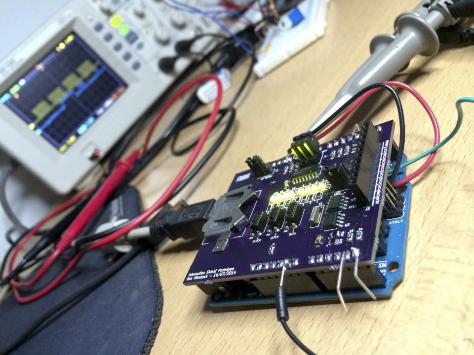
August 18, 2014
Huge amount of ripup today. I modified the schematic to clean it up a bit, added 3V3 and 5V to the ADC pin header, moved all the components topside, freed up a couple of PWM pins for end user availability, verified that the debounced buttons were available for digitalRead, moved the battery down to free up topside copper space… and now have to, essentially, reroute the entire board from scratch. Is what it is.
* * *
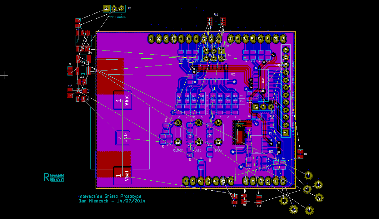
Marathon layout and routing session in the books. Board says 5 nodes are still disconnected, one of which is a “dammit I painted myself into a corner” with the top side copper, where I have a little island of 5V that is disconnected from the power plane because of oodles of signal traces. The amount of vias seems large to me, and I keep telling myself it’s because I moved everything top side on a two sided board, so consequently, I have to do a bit of nutty routing to get everything connected AND allow the power / ground planes to pour fairly consistently. Anyway, it’s 12:45AM and I’m bushed. I’ll finish this up in the morning.
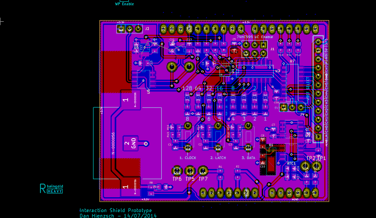
August 19, 2014
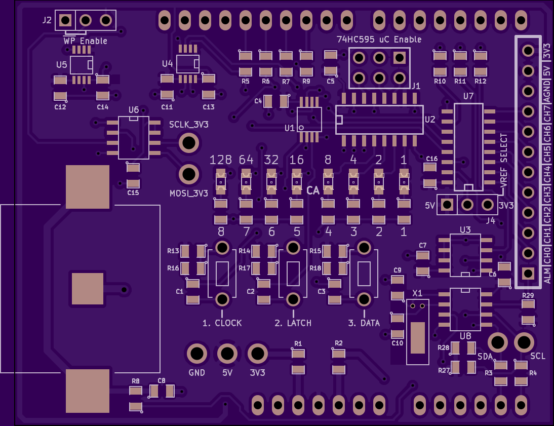
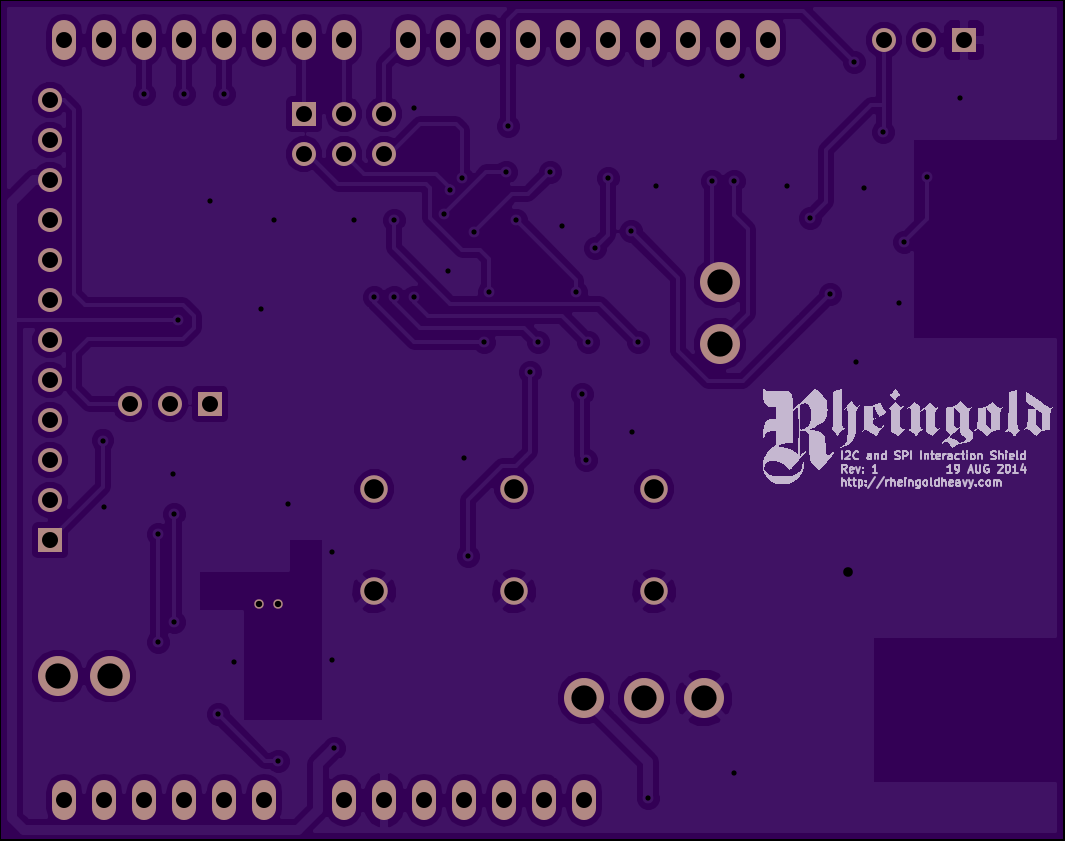
Cleaned up the rest of the routing. Had a few disconnects because of the small pad spacing on the LSSOP footprints, but fixed it by running little traces back into the 5V copper pour. Then spent a dumb amount of hours trying to put the Rheingold Heavy logo into the backside copper before I realized what a waste of time it was for a prototype board and just put it back in the backside silkscreen.
Need to double check the SOIC16 footprints still, and generate / review the gerbers.
* * *
Yep, the 8-pad vs. 16-pad footprints were different. In KiCad, the footprints are SO8E and SO16E respectively. Here’s what I found…
|
1 2 3 4 5 6 7 8 |
SO8E PAD SIZE X: .0236 PAD SIZE Y: .0551 SOLDER MASK RELIEF: GLOBAL PAD SEPARATION X-AXIS CENTER-CENTER: .050 PAD SEPARATION Y-AXIS CENTER-CENTER: .210 PAD SEPARATION Y-AXIS INNER EDGE - INNER EDGE: .155 PAD SEPARATION Y-AXIS OUTER EDGE - OUTER EDGE: .2652 |
|
1 2 3 4 5 6 7 8 |
SO16E PAD SIZE X: .020 PAD SIZE Y: .045 SOLDER MASK RELIEF: GLOBAL PAD SEPARATION X-AXIS CENTER-CENTER: .050 PAD SEPARATION Y-AXIS CENTER-CENTER: .200 PAD SEPARATION Y-AXIS INNER EDGE - INNER EDGE: .155 PAD SEPARATION Y-AXIS OUTER EDGE - OUTER EDGE: .245 |
So I had to increase the pad sizes by a smidge, then push everything out on the Y-axis .005″ from the centerline and now it should be a little easier to solder.
* * *
Proofed the gerbers, saw a bunch of silkscreen problems that had to be fixed… uploaded to OSHPark, saw more problems… rinse… repeat.
Order placed for Rev 1!
