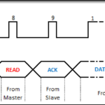
Each component you will encounter that communicates over a serial connection, will require understanding the timing of those interactions. Timing diagrams attempt to break these parts up in a way that allows you to understand what needs to be sent or received and in what sequence that needs to happen. Mind you, timing diagrams attempt to do this, sometimes very well, sometimes not so very well.
Objectives
- Understand what the purpose of a timing diagram is.
- Recognize typical symbolic conventions in timing diagrams.
Background
No previous reading is necessary for this module.
Schematic
There is no schematic associated with this module.
Setup
No hardware is necessary to understand this module.
What is a Timing Diagram
Timing Diagrams are a way to symbolically represent the activity of one or more signals being transmitted or received by a component, and the way they relate to each other over a span of time. Any device that communicates with other devices over serial communications methods will include them in their datasheet. At their best, they can be used to quickly visualize what needs to happen in order for a successful transmission or reception to occur, at their worst, they further obfuscate what is most likely already a very occult specification. Your goal as an engineer, is to pull the layers of the diagram apart to see what steps you’ll need to perform when designing your schematic and assembling your code.
For a basic example, let’s take something we already know and build a diagram around it: we’ll build out a timing diagram that describes how to use the buttons of our 74HC595. As a timing diagram specifically deals with the sequencing of steps, you’ll invariably find the clock signal at the very top, because that is what governs the rise and fall of your signalling empire.
Below the clock signal, each of the other necessary signals are listed, vertically synchronized with the clock signal at the top to show you what the end result of a particular signalling sequence is. To start with, we’ll need to see the clock, data, latch, and qa output signals.
We have our signals listed, so now let’s begin diagramming the interactions out. It all starts with the clock. We have several functions that we want to express in our diagram…
- How do you clock in a zero?
- How do you clock in a one?
- What happens on the outputs with multiple clock cycles?
Starting at the top… let’s diagram the steps necessary to clock in a zero. We’ll need to show the clock going high, the data staying low and the latch cycling.
In this diagram, we see that the latch must come after the clock, because that is how they are vertically synchronized. We also see that if nothing occurs on the data line, then we’ve not done anything particularly interesting, seemingly.
Now let’s show what happens when we clock in a one. We’ll need to now show the clock going high, the data going high, the latch cycling, and the affect on the output.
Again, we look immediately for the sequencing of steps. We see that data is high before the clock goes high, indicating that the clock is positive edge triggered. We also see that after the clock and data have done their thing, that the latch changes the output, indicating that the one has been clocked in, and that the output changes on the positive edge of the latch signal. Further, given no other changes, qa out will remain high. That’s a lot of information to convey in four little lines.
Let’s add another output, qb out, and clock in another zero, to indicate that this is a shift register.
The diagram now shows the shifting of the zero into QA, resulting in its output being shifted into QB, and all of that being triggered by the cycling of the latch. We can show this movement of the lone one through our shift register by listing the remaining outputs and sequencing it all out.
There’s an awful lot of extra space in between the pulses that makes it a little easier to see the segmentation of time versus each of the signals, but that white space can be removed to capture all the action in a much tighter area.
Obviously Texas Instruments uses some form of word processing software to generate their timing diagrams and I use a javascript web plugin, so the images won’t match exactly, but here is a copy of the timing diagram from the 74HC595 datasheet…
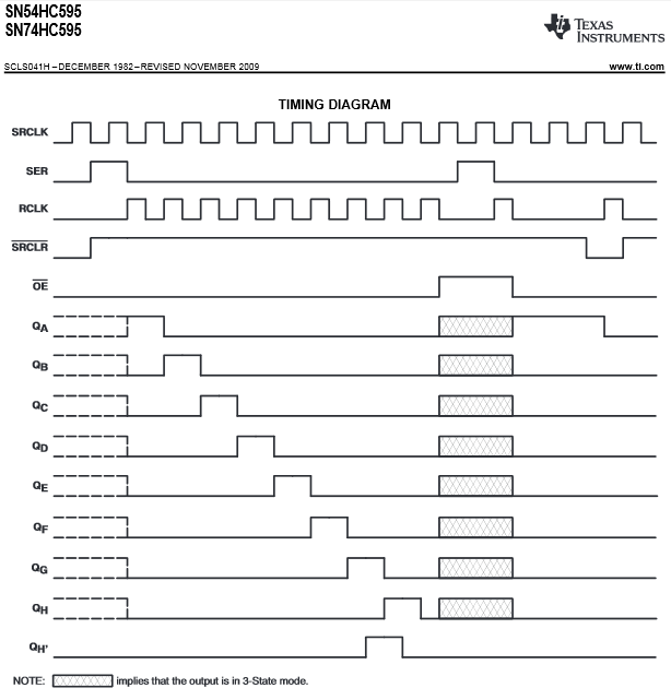
The official datasheet contains information related to pins that aren’t really being used on the Education Shield (remember our diagram only reflected what the buttons did), but hopefully, the official diagram should make sense when you look at it now. The major differences are at the beginning of the outputs, where the lines are dotted indicating an unknown state of the outputs because SRCLR is held low (the javascript plugin can’t do dotted lines), the section at the end, where output enable is brought high, and the outputs go into the “third state” of high impedance, denoted by the greyed out area, and finally, the addition of the QH’ serial data pin used for daisy chaining shift registers together.
Typical Timing Diagram Graphics
Here is a list of typical graphics that you’ll see in timing diagrams and their usual definitions. These aren’t standardized so you may see some, you may not, you may see them used in other ways, but generally speaking these are typical, and conform with the datasheets you’ll use with the components of your Education Shield. The names I’m using are my own, because I don’t know of any other page like this on the internet. I should totally name one of these signal symbols after myself.
Square Wave
This indicates a very constant signal, usually associated with the clock. You will typically find the clock at the top of the timing diagram as mentioned above. It is customarily used when presenting the overview of a timing sequence, for example, showing when the Chip Select needs to go low for an SPI trigger, rather than the specific events occurring during a single clock cycle.
Arrows indicating positive / negative edge trigger
The arrows very simply indicate where the signal is triggered, either on the positive going edge or on the negative going edge.
Ramping Signal
The ramping signal is usually shown for detailed timing, such as that surrounding a single clock cycle. Generally it’s used to show that something is occurring due to edge triggering of some sort, or to make it very clear that two signals are in direct opposition.
Either-Or (this should totally be the “Rheingold” signal)
The Either-Or signal is the sideways criss-crosses in the diagram above. It represents that the value of the corresponding signal can be either high or low for the clock cycle that is sampling it. This is typical of a data line, where the values are dictated by external events and the data line is merely sampled by the clock signal on the leading or trailing edge.
Greyed Out
There can be several definitions associated with a greyed out section in a timing diagram, however it is most often used in the event where the processing system simply doesn’t care what the values are. SPI and I2C interchanges on our Arduinos are always 8 bits in length, but if you have some value you need to specify that isn’t a full byte long, the datasheet will say something like, “the three MSBs contain the configuration and the remaining 5 bits are dummy data”. Another typical definition for the greyed out area is describing a change in the state of a pin, such as when the output enable pin on the 74HC595 goes high, and the outputs change to a high impedance state. If the datasheet intends to describe a state change, it is usually included in footnotes for the diagram so you aren’t confused (too much).
“Time Passes” spacing
The little gap in the middle is used to indicate that a significant amount of … something… is occurring. In the case above, you might be clocking in a bunch of data. For example, the flash RAM on the Education Shield is able to send out up to 256 bytes at a time, and it would be indicated using the bit labeling below with the “time passes” gap here.
Bit Labeling
Bit labeling provides greater detail to explain what the specific contents is of a series of values, or as in the example above, to show that you can stream data out. This is used generally to indicate the position of one type of data chunk, such as address or configuration bits in relation to other chunks of bits in a data stream.
Arrows and Space Demarcation
This is typically where a timing diagram goes from being a help to being a hindrance. If you’re lucky, the timing diagram designer will have found a way to cram as much text into the page as possible. If you’re not lucky, it will only reference numbers that lead to footnotes at the bottom of a table four pages before or after the diagram itself. In the example above, the diagram drawer is showing that the first three bits are address bits and the next five bits are all data bits.
This page uses the fantastic Wavedrom javascript utility located here on GitHub.