Managing the Bill of Materials (BOM – pronounced “bomb”) for a project, even a small one, can get unwieldy fast. If you’re talking about hand assembling even two or three boards, it can be tricky keeping track of how much of any particular part to order. Then you discover that one of your parts is out of stock and you need a replacement, but it’s a different size, so now you update the footprint, but did you update it in the spreadsheet you’re using as a parts list? This is chaos, and we need to bring order to it, by using our EDA tool. Here at Rheingold Heavy, we’ve standardized on KiCad BOM management.
KiCad BOM Management – A Little Back Story
Last year, I designed, prototyped, tested, iterated and sold (via Kickstarter), the I2C and SPI Education Shield and it’s matching I2C Display Addon. Using my old tried and true method of BOM management, I started a spreadsheet to keep track of every entry in the schematic. Color coded, descriptive headers, even checklists for verifying footprints against datasheets. It was great. At first.

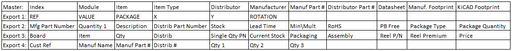
As you can tell, by looking at the columns, I’ve had to hide some rows just to get it to fit on the screen to take a screenshot. So while it’s certainly detailed, it’s labor intensive to maintain.
As I would discover, when you need to send your BOM to contract manufacturers and assembly houses, they all want a piece of that file, but they all want it in different formats: XLS, PDF, CSV, you name it. Then, as you start to get quotes back, the manufacturing process feeds back into the design and you need to make some modifications. For example, Small Batch Assembly, which I chose to perform assembly for Kickstarter fulfillment, had a list of assembler supplied parts, which they are able to furnish at volume price levels way below what I can buy at as a single entity. However, the board was all 0805 passives, and SBA’s component list is all 0603. Well, back into the design I go and start updating. Well, it was very apparent that I was starting to get confused between the CSVs I was using for manufacture, and the master BOM I was trying to maintain in Excel. And then it came time to buy parts, and getting quotes from distributors means another round of BOM exports, all formatted with different column headers and information… and then you make modifications to those, but is that being fed back into the master BOM and the manufacturer’s BOM?
And then a production approved part went End Of Life. And then a different production part when Out of Stock. It was an absolute mess, and I managed my way through it only by being willing to quintuple check every single last thing before I pressed the “Production Run” button. And I still screwed up a footprint, which fortunately only cost me about $100 to rectify.
The Solution
Every item that is essential to maintaining an immaculate BOM can be managed inside KiCad. What I’ve decided to document here, is the workflow I’m following for back-filling an old schematic with the values necessary to use it as the central repository of all things Bill of Materials. Either you, as the reader, are in the same boat I’m in and that’s why you’re reading this, or you’re looking to head this pain off at the pass, and that’s why you’re reading this. Either way, it should be helpful.
Here are the problems we’re trying to solve…
- Every BOM customer (distributors, CM’s, etc) seemingly want different information.
- Some field values in KiCad aren’t captured in my spreadsheet and viceversa.
- Some field values that ARE in KiCad, don’t match the expected CSV field values at various distributors.
- There is no way to maintain component pricing data in KiCad.
- It seems that every time I need to upload a BOM to someone, I have to reinvent the wheel.
Let’s approach this as any other engineering challenge and set some design goals for us to work towards…
- Determine what information needs to be captured and maintained.
- Determine where it will be located within KiCad.
- Assign field names to the data items so that they can be understood as CSV file headers without editing.
- Ideally, ensure that a single export of the BOM can be immediately uploaded into OctoPart for quick budgeting.
- If additional massaging is necessary for parts distributor upload, do it via Macro and not manual action.
I think the five design goals match well against the five pain points, and if we can find solutions to each of them, that result in being able to eliminate confusion, errors, inaccuracies and uncertainty, then we’ve gotten over a major hurdle between design and production.
What Information Needs To Be Maintained
Recently, Chris Gammell posted a link to The Amp Hour subreddit, discussing this exact topic. It was a blog post from Spark entitled “Creating and Optimizing a Bill of Materials“. The good news is, inside that blog post is a pretty comprehensive list to choose from. If you follow the link inside it to Bunnie Huang’s blog, he even gets into greater detail with Minimum Order Quantities (MOQs) and Lead Time specs. I don’t need to capture all of that information for my purposes, because I’m not manufacturing in the 1000 and 10,000 quantities where this becomes crucial, so I’ll take what I want and leave the rest, like a salad bar.
Here are the items I already collect in my schematics (which for reasons that are beyond me, I decided not to use when designing the I2C/SPI Shield).
| Field Name | Description |
|---|---|
| Reference | Default field, auto-populated by KiCad during annotation |
| Value | Default field, filled in manually when laying down a part |
| Footprint | Default field, either manual or backfill from CvPCB |
| Datasheet Link | Self explanatory |
| MFN | Manufacturer's Name |
| MFP | Manufacturer's Part Number |
| S1PN | First Source Part Number |
| S1PL | First Source Part Link |
| S2PN | Second Source Part Number |
| S2PNL | Second Source Part Link |
The first three are defaults, and the next three are pretty obviously important, but I’m going to ditch all the sourcing information. I’m buying parts from either the usual suspects (Digi-Key, Mouser, Avnet, etc) or from the CM themselves, if they have common parts pre-loaded on their pick-n-place. The goal will be to output something that can go immediately into Octopart, allowing me to find suppliers quickly anyway.
So what are the most important things to capture in addition to that? I’m going to add (stealing mostly from Spark’s list)…
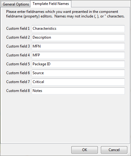
| Field Name | Description |
|---|---|
| Characteristics | Voltage / Current / Tolerance specs. Fortunately, this is basically the "description" field at any distributors website, so you can just paste it in. |
| Description | I can't even begin to imagine why I don't have this as a field in my schematic components already. I can save myself a field and prepend each description with a short subsystem descriptor for ease of CSV sorting. |
| Package ID | I'll put the JEDEC footprint name in here if I can find it, or the closest approximation provided by the manufacturer. |
| Source | Here is where I'll communicate if I'm happy with whatever part they can find to match the Value field, or if I need them to find the MFP I list. Two values should go in there: ANY / SPEC. Any means, use any matching part. Spec means, use the specified part. |
| Critical | Just a little field I can put an "X" in, if I want to ensure I don't just gloss over it when communicating with CMs. |
| Notes | Any information I want to let future me know of when he looks back on the design and wonders what was going on. |
That’s 12 pieces of information that need to be captured (including the defaults). For every… single… component. If you think that sounds tedious, you’re right. If you think that sounds like a pain in the ass, you’re right. If you think that it isn’t absolutely critical, you need to by me a beer so we can talk about it.
Adding Custom Fields To Components in KiCad
The first thing you should know, renaming any of these custom fields in KiCad will potentially wipe out any entry you have there, in any schematic you open in that install, period. So be very, very careful about what you are about to undertake. If there are custom fields already noted in other schematics, that you want to keep, then you’ll have to work within that very specific constraint. The custom fields are specified at the application level in eeSchema, not on a schematic file basis. There are no schematic level custom fields, unfortunately. You can add extra fields beyond the eight allowed in the options below, but those are component level only, and they don’t play well with export — they just get tacked on after whatever the last field is you had, even though it should technically appear in the ninth field.
Open up eeSchema, and under Preferences, go to Options…
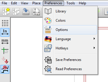
That will open up a small configuration window and you want the second tab, “Template Field Names”. This is where you will enter the extra information you want to capture.
Back Filling Specifications
Well, here’s what I have to do now. The I2C/SPI Education Shield schematic has 73 parts, which, after reordering and naming the custom fields, have no specifications beyond “Value” and “Reference”. I know R7 is 22K, but that is the only bit in there. So now I need to go in and edit each and every single component and populate that data. I’ll be back when I’m done and let you know how long it took.
Not too bad. It took me about 3 hours, and I developed a couple of tricks along the way to help keep track of things.
- Because of a bug in KiCad’s export system, you have to put something into every custom field for a component, or that field will be ignored on export, and the next field moved into it’s place, and they shove all the empty fields to the end, which screws up the formatting. Just drop a space or a “~” in it to mark it as empty. Consequently, I changed the “Critical” field from a simple “X” to “Y” or “N” instead.
- Obviously, it’s easiest if you do all of this stuff at the beginning, when you’re first spec’ing out your components. When you settle on one, fill in the details as you go, and the pain is negligible. However, while doing a new design, or back filling like I just did, a life saver is the fact that KiCad transfers the full contents of the custom fields when you copy a component — it just drops the reference designator to “?”. So, when I went in to change the eight current limiting resistors connected to the LEDs, I just fully completed the first one and then replaced all the others with copies. However, it is critical that you immediately manually restore the original reference designator, or you will break the association with the foortprint! Of course, you can have two components with the same ref right next to each other in the schematic, and as long as you don’t generate a netlist, you’re cool. So copy, move them next to what they’re replacing, rename the reference, then delete the old one and drop in the copy.
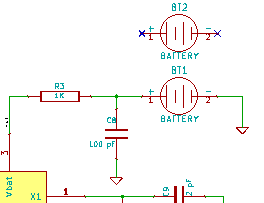
- I realized that I had two full sets of specs for the battery… the battery itself, and the battery holder, but it only appears once in the schematic. It dawned on me that I can put anything I really want in the schematic and have it be tracked. If I don’t associate a footprint with it, it will never interfere with the PCB Layout. So I spec’d out the original battery component as the Harwin S8211 battery holder, since it is electrically connected with footprints, but added another battery component right above it, with little blue “X” “no connect” markers on the pins and filled in the CR2032 battery information. I also added disconnected jumpers next to all the male pin headers, so that the shunt jumpers will be tracked as well. This will cause a re-annotation when you export the netlist, so be very, very careful selecting the parameters of your annotation: make sure you’re only annotating NEW components, not overwriting existing.
- It would be wise to save repeatedly as you go. When you’re done, make sure to do a bug check in eeSchema. Then export the netlist and view it in CvPCB. If you suddenly don’t have any footprints associated anymore, then you probably messed up an annotation somewhere along the way and you are, basically, screwed 🙁 But you’re a smart sort of person who doesn’t make mistakes like I do, and you’ll have everything as it should be. Open up PCBNew and import the netlist to make sure nothing went wacky. If something DID go wrong when you look at your layout, DO NOT SAVE. Just Exit Without Save, go back and fix whatever needed fixing and do it again until it’s right.
- With regard to hose loose parts, like the shunt jumpers and battery, it might be wise to create a separate hierarchical sheet in your schematic called “Loose Parts” and just tuck all of that stuff in there to keep track of it
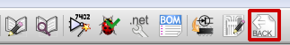
The final step to getting your components fully detailed, is to back fill all the footprint data, after you’ve completed your footprint assignments in CvPCB. This is a little awkward just because of the wording they use in the dialog boxes, so we’ll take it step by step.
Click on the “Back” button to import your CvPCB footprint assignment file…
… you’ll be asked to select your .cmp file. Grab it and click “Open”. You’ll get a funky dialog box that opens up saying the following…
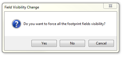
Allow me to translate: “After importing, would you like to apply a global visibility setting to all the component footprint fields?” If you select “No”, then whatever the current visibility setting is will be used and the import will be executed. If you select “Yes”, then you are given a second dialog box…
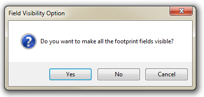
If you select “Yes”, all the footprint values will be visible for every component in your schematic. If you select “No”, all the footprint values will be invisible for every component in your schematic. Choice is yours, but I think it adds a lot of purple distraction to the schematic if you make it visible. The fortunate thing is you can go through this process over and over again, import + visibility enable/disable, if you want. It won’t mess anything up.
Next Steps
We now have exceptionally detailed component information in our schematic. It is on us now to maintain that data whenever we make a change. If you get into the habit of it though, I think you’ll find management of your component level information much easier to deal with.
Next we want to deal with the exported data. We’ll cover that in Part 2.
For more KiCad tutorials, Click Here.