In this module we’ll begin working with the very fundamentals of serial communications, using the shift register and buttons on the Education Shield to develop our understanding of clocks, data input and latches.
Objectives
- Understand what a shift register generally does
- Understand the function of clock, data and latch
- Understand what the correct sequence for sending and committing data is and why it works
- Familiarize yourself with the terms “MSB”, “LSB”, “clocking in”, “clocking out”, “latching” and “edge triggering”
- Practice manually sending data to the shift register using the CLOCK, LATCH and DATA buttons.
Digital Logic Basics Part 1
Digital Logic Basics Part 2
Digital Logic Basics Part 3
Digital Logic Basics Part 4
Digital Logic Basics Part 5
Shift Register Basics
Schematic
Education Shield – Shift Register Subsystem
Setup
For this module, you’ll need the following equipment:
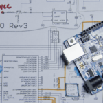
- Education Shield or the Manual Serial Communications Trainer
- Arduino UNO R3
We want to assemble the system in a way that ensures that your Education Shield is only receiving power from the Arduino and no signalling – you will provide the data, clock and latch signalling manually.
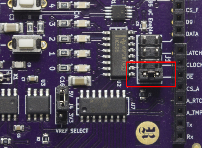
1. Remove all the jumpers, except for the OE Jumper, from the 74HC595 Enable block along the edge of the Education Shield. This will disable microcontroller interaction with the shift register clock, data and latch pins, ensuring that the buttons have exclusive control.
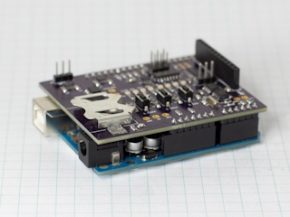
2. Mate the Education Shield with your Arduino UNO R3, to provide the 5V and ground.
3. Finally, connect your Arduino to your USB cable, and upload this little sketch to drive the OE pin low.
|
1 2 3 4 5 6 7 |
void setup() { int oePin = 5; pinMode (oePin, OUTPUT); digitalWrite (oePin, LOW); } void loop() {} |
Alternatively, you can use the Manual Serial Communications Trainer instead. Connect 5V and CLR to 5V, GND and OE to GND, DATA to D8, LATCH to D7, and CLOCK to D6. No code is required.
Serial Communications Fundamentals: Clock, Data, Latch
A register is a single chunk of electronics memory, and one we will become very familiar with over the course of working with I2C and SPI. The 74HC595 shift register is a register into which data is loaded sequentially, one bit at a time, and for every bit that enters, one is forced out — “shifted” out. The register is 8 bits wide, meaning you can store 8 individual ones or zeros in it at any particular time. The important thing to remember is that the shift register is kind of like Electronics Thunderdome: one bit enters, one bit leaves. The bits going in, are our data.
Sending and receiving data is the whole point of serial communications fundamentals. Much like human speech, where we need to include pauses and full stops to indicate when our point has been made, or when we’re ready for some form of response, the language of serial communications relies heavily on appropriate timing. We are going to start to explore this using a Texas Instruments 74HC595 Shift Register, which incorporates three separate signals to perform its communications: clock, data and latch.
A clock signal is the basic building block of all the timing that occurs during a serial transmission. It is the thing that chops a bunch of high and low pulses of (usually) unequal lengths into defined, individual, ones and zeros. Typically, our hope is to send and receive those ones and zeros as fast as we possibly can, but for now, we are going to slow it down to the speed of the typical human: whole seconds instead of nanoseconds.
The data signal is that bunch of high and low pulses that needs to be accurately chopped into defined lengths. Every time your clock signal pulses, your electronics system is going to sample the state of that data signal to determine whether it’s a one or a zero. There are many different standardized values for what constitutes a one or a zero (the beauty of standards being how many of them there are), but in the world of our Arduino Uno we are going to interpret a 0 to be ground and 1 to be 5V (at least until we get to talking about the Flash memory chip).
The latch signal functions like the period at the end of a sentence; it tells the shift register when the talking has ended. Unfortunately, the shift register is like a disinterested party guest who’s attention span is only sufficient to remember the very last thing you said after you stopped talking. If you don’t stop talking, the ones and zeros will go in one ear and out the other of the shift register, and all but the last 8 bits of your communications are lost. This isn’t necessarily a bad thing: 1) just control how much data your sending each time and keep it to 8 bits if you can, and, 2)avoid idiots like that at parties.
Working with the Shift Register
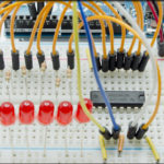
When you first applied power to your Education Shield, all eight of the green LEDs light up in the default state for the shift register. Below those LEDs, are the three buttons labeled as “CLOCK”, “LATCH”, and “DATA”. Each of those buttons is designed to send a very clean 5V to its matching pin on the shift register as long as you hold the button down; release the button and the pin goes back to ground (0V).
The shift register works by taking the level of the data pin on the rising edge of your clock signal, and loads that into a buffer. If the data pin is at 5V when the clock signal goes high, a one is saved to the buffer. If the data pin is at 0V, then a zero is saved to the buffer. The concept of the rising edge of the clock is important: even if the clock signal stays high for 20 minutes straight, and the data pin pulses away like crazy, if it wasn’t high at the moment the clock transitioned low to high, then that data is lost. That is what is referred to as edge triggering, and it can occur on the rising edge or the falling edge of a clock signal. By using edge triggering, the chip designer is making sure that the moment at which the data signal is sampled, is very, very precise.
Each time the clock goes high, it is commonly referred to as clocking in a bit of data. The size of the data buffer of this shift register is 8 bits, so it can store 8 ones or zeros in the order they are clocked in. If you clock in a ninth bit, the first of the initial 8 bits you sent is forgotten. Or is it? A feature of the 74HC595 is that they can be daisy chained together, and using a common clock signal, you can connect the data out line of one 595 to the data in of the next 595. Each bit that is pushed out of the buffer of the first shift register — clocked out of the first shift register — is subsequently clocked into the second one and on down the line. (There’s only one shift register on the Education Shield, so you’ll have to build that circuit yourself to see it in action.)
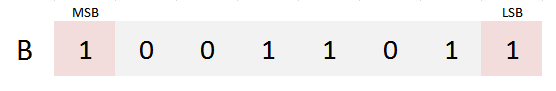
It is important to also know which direction the data goes in. Think of the shift register as a train car with eight windows; when the passengers get on, do you see them moving past the windows left to right, or, right to left. The order in which our bits go into our passenger train is called most significant bit first or least significant bit first. When you look at a byte of data, 8 bits of data, the bit on the far left is called the most significant bit and the bit on the right is the least significant bit. Let’s take the example of the binary value B10011011:
Knowing what this means key to the fundamentals of serial communications: you have to know how data is going to be fed out of your chips, and you need to know how data is fed into your chips — which way are the passengers moving in the train car. If the chip you’re working with is expecting “MSB first”, and you send it in LSB first, you are submitting an entirely incorrect value.
The way the chip expects to send/receive data is always specified in the datasheet in some fashion. In the case of our 74HC595, the bits flow in alphabetical order: the pins are labeled “OUTPUT A”, “OUTPUT B”, and so on. This can be slightly confusing. If you clock in a single 1, it will be sent to Output A, but what “A” represents is entirely reflective of your design: it could be the right-most LED or the left-most LED or to the three o’clock position in a circle. For our purposes, the LEDs are connected right to left: HGFEDCBA, to accurately reflect the pattern of a byte of data. Therefore, bits enter on the “right” and move to the “left” and you are clocking in the MSB first, and sending the remaining bits in sequence. B10011011 would be sent as : 1, 0, 0, 1, 1, 0, 1, 1. (When you look at the datasheet for the chip though, the phrase “most significant bit” doesn’t appear anywhere in there, and it doesn’t explicitly state that a bit clocked in first appears on output “A”, even thought that seems somewhat elementary. You confirm this by reading the timing diagram, which will cover in another module.)
The final act necessary to commit the bits we’ve sent to the shift register, is to cycle something called the latch. The buffer of the shift register is called, literally, “the shift register” and the actual output is called the “storage register”. You shift bits into the shift register all day long, but until you apply the latch, it isn’t committed to the storage register. The mechanism of the latch, is just a series of master-slave logic gates that only allow the values in the master to pass to the slave when a specific input, the latch signal, goes high. Since the commit occurs on the high going signal, the latch is positive edge triggered. If you leave the latch in a steady state, low or high, nothing will ever change on the outputs of the register. It’s the transition from low to high that commits the values in the shift register to the storage register.
Playing with the 74HC595
Your Education Shield should have all 8 LEDs turned on at this point. Our initial goal is to turn all the LEDs off.
Let’s start by clocking in a single zero. You do this by simply pressing the CLOCK button once. That will raise the voltage at the SRCLK from 0V to 5V. After you press it, nothing has seemingly changed, because you haven’t committed the value to the outputs. Do that now, by pressing the LATCH button, which will raise the voltage on the RCLK pin to 5V, supplying the rising edge trigger necessary. The right most LED has now gone out.
The clock signal went high, but since you weren’t pressing the data button as well, you clocked in a zero, and then committed it by cycling the latch. That means the LED on the far left got shifted out because you shifted in a zero on the right.
Now, let’s do the same thing again, except press the CLOCK button twice. Again, nothing will seem to have changed until you press the LATCH button. Two more LEDs have gone out because you’ve shifted in — clocked in — two zeros.
Let’s turn off all the remaining LEDs by pressing CLOCK an additional five times, then pressing LATCH.
The Education Shield looks rather dull without any of the LEDs twinkling, so let’s start turning them back on. The instructions can be read by hovering your mouse over the box below, but see if you can figure out how the button presses should work on your own to turn the first LED back on. The key to remember is that the clock samples the state of the data line on the positive going edge.
Hover to read answer
If all went well, you should now have a single LED burning brightly on the right most position.
What sequence of buttons would be needed to light all the LEDs again.
Hover to read answer
Clocking in a Full Byte
Remember, the irritating party guest only remembers the last eight bits of data, so as long as you’re sending eight bits at a time, a full byte, that’s what will be committed to the output when the LATCH button is pressed. Let’s practice clocking in some full bytes then.
This LED pattern is B10101010.
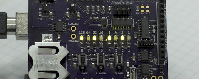
How would you clock in B10101010?
This LED pattern is B00011000.
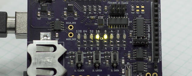
How would you clock in B00011000?
This LED Pattern is B10010101.
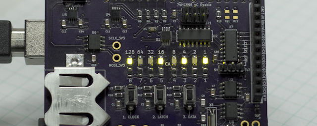
How would you clock in B10010101?