We can Read and we can Write, so now let’s talk about erasing AT25SF081 memory…
Objectives
- Understand what a block is.
- Understand what block sizes can be erased.
- Determine which opcodes are used to erase various block sizes.
Background
AT25SF081 Tutorial 02: Reading Memory Byte
SPI Signals
Adesto AT25SF081 Datasheet
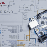
Schematic
Education Shield – AT25SF081 Flash Memory Subsystem
Setup
For this module, you’ll need the following equipment:
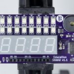
- I2C and SPI Education Shield or the AT25SF081 Flash Memory Breakout Board
- Arduino UNO R3
1. Mate the Education Shield with your Arduino UNO R3. If you’re using the AT25SF081 Flash Memory Breakout Board, connect 5V to 5V, 3V3 to 3.3V, GND to GND, HOLD to Digital09,CS to Digital10, MOSI to Digital11, MISO to Digital12, and CLK to Digital13. That’s a lot of pins!
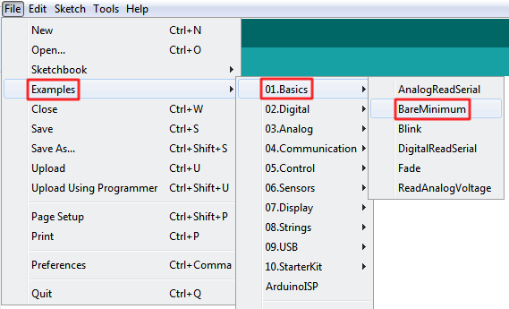
2. Connect your Arduino to your USB cable, and use the Arduino IDE to upload the “Bare Minimum” sketch from the Basics section of the Examples.
Working with the HOLD pin is not necessary for any of the tutorials, it is only included on the breakout board for completeness. In the sketch it will always be set as an output in a high state, and on the I2C and SPI Education Shield, the pin is tied directly to the 3V3 rail on the PCB.
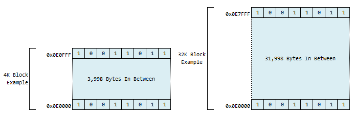
Memory Array Blocks
Similar to how the bytes of your memory array are arranged in pages when you program the AT25SF081, the erase commands deal with arrangements of bytes called blocks. The block sizes comprise 4K bytes, 32K bytes or 64K bytes in size, and each block size has an associated erase opcode associated with it. If you’re feeling really frisky, you can erase the entire chip at once as well using that dedicated opcode.
- 4K Erase: 0x20
- 32K Erase: 0x52
- 64K Erase: 0xD8
- Chip Erase: 0x60 or 0xC7
Arranging the bytes into blocks allows for faster erase times and simplifies the internal structures of the chip. If you think back to what it takes to make a crude single bit register using discrete logic, imagine that on a scale of millions and you’ll swiftly see the amount of stuff that would have to be crammed into a chip that small in order to allow erasing each byte of memory individually.
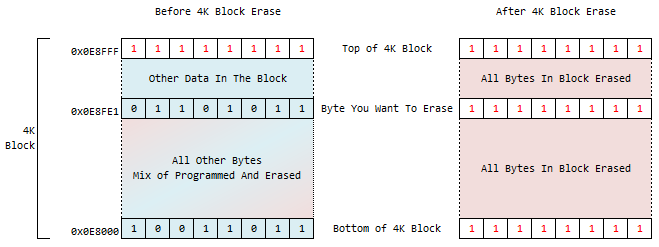
Since erase operations occur exclusively on a block level, that means choosing to erase a single byte, regardless of where it appears within that block, will cause the entire block to be erased with it. Just like you need to be cognizant of how much data you want to program to the byte and where you’re starting to write it to with a mind to avoiding problems with overwriting data within a page, you have to be aware of what other data is vulnerable within a block of memory when you apply one of the erase opcodes on it.
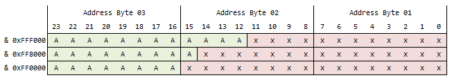
Just like the read, and program commands, the erase commands necessarily requires you to supply a starting address for the operation. However, unlike the others which start at the specified byte, the erase opcodes will interpret any of the least significant bits that correspond to some address in the middle of the block, as zero. This forces the command to always be executed at the starting threshold of the block.
In the example below, you can see that a starting address of 0x0E8FE1 was used for the 4K erase command, but the chip does the equivalent of logically anding that address with 0xFFF000 to only keep the parts of the address that indicate the start of that block.
For a 32K erase, the internal logical and mask would be 0xFF8000.
For a 64K erase, the internal logical and mask would be 0xFF0000.
Writing a Function for Erasing AT25SF81 Memory
The code to erase blocks of the chip is very nearly the same as that used to program the chip. You first set the WEL bit, then send the erase opcode for the size you want to zap, and then the starting block address. That’s all. As soon as you bring the chip select pin high after sending the block address, the chip will begin the erase cycle.
|
1 2 3 4 5 6 7 8 9 10 11 12 13 14 15 |
void erase_4Kblock(long eraseAddress) { digitalWrite (CS_AT25SF081, LOW); SPI.transfer (OPCODE_WRITEENABLE); digitalWrite (CS_AT25SF081, HIGH); digitalWrite (CS_AT25SF081, LOW); SPI.transfer (OPCODE_04K_ERASE); SPI.transfer ((eraseAddress & 0xFF0000) >> 16); // Byte address - MSB Sig Byte SPI.transfer ((eraseAddress & 0x00FF00) >> 8); // Byte address - MID Sig Byte SPI.transfer ((eraseAddress & 0x0000FF) >> 0); // Byte address - LSB Sig Byte digitalWrite (CS_AT25SF081, HIGH); } |
All you have to do is shoehorn that function into the code from the program tutorial (in this case I have replaced the program code with the erase code) and the sketch is ready to go.
|
1 2 3 4 5 6 7 8 9 10 11 12 13 14 15 16 17 18 19 20 21 22 23 24 25 26 27 28 29 30 31 32 33 34 35 36 37 38 39 40 41 42 43 44 45 46 47 48 49 50 51 52 53 54 55 56 57 58 59 60 61 62 63 64 65 66 67 68 69 70 71 72 73 74 75 76 77 |
/* A sketch to erase a 4K block of the 8-Mbit AT25SF081 Flash Memory IC. This sketch will erase a 4K block of memory specified by the some24bitLocation variable within Setup. The code supposes the use of the Education Shield, but if you're using a breakout board, connect the CS pin to Digital 10, HOLD to Digital 9, and the SPI pins in their usual locations. Website: https://rheingoldheavy.com/at25sf081-tutorial-05-erasing-memory Datasheet: http://www.adestotech.com/wp-content/uploads/DS-AT25SF081_045.pdf */ #include // Include the SPI library SPISettings AT25SF081(8000000, MSBFIRST, SPI_MODE0); // Sets the pin values for the AT25SF081 and MCP3008 const int CS_AT25SF081 = 10; // Flash Memory Chip Select - Active Low const int holdPin = 9; // HOLD Pin - Active Low // Set bits for the various Flash IC OpCodes (see datasheet) const byte OPCODE_SLOWREAD_ARRAY = 0x03; // Memory read up <= 50Mhz (see datasheet) const byte OPCODE_FASTREAD_ARRAY = 0x0B; // Memory read up <= 85Mhz (see datasheet) const byte OPCODE_WRITEENABLE = 0x06; // Enable programming const byte OPCODE_PROGRAM = 0x02; // Write command const byte OPCODE_READSTATUSREGISTER01 = 0x05; // Read Status Register 01 const byte OPCODE_04K_ERASE = 0x20; // Erase a 4K block const byte OPCODE_32K_ERASE = 0x52; // Erase a 32K block const byte OPCODE_64K_ERASE = 0xD8; // Erase a 64K block const byte OPCODE_CHIP_ERASE01 = 0x60; // Erase whole chip const byte OPCODE_CHIP_ERASE02 = 0xC7; // Erase whole chip const int programButton = 7; // LATCH button used to set resolution void setup() { Serial.begin (9600); pinMode (programButton, INPUT); AT25SF081_init (); Serial.println ("Press the LATCH button to execute the ERASE command..."); Serial.println (); } void loop() { int buttonPressProg = 1; // Determins if this is the first button press long some24bitLocation = 0x000000; // Starting address we'll use to R/W byte someData = 0xFF; // Some data to write to memory byte pageData[256]; // Array of bytes to hold a page of data while (digitalRead(programButton) == HIGH) { if (buttonPressProg == 1) { buttonPressProg = 0; SPI.beginTransaction (AT25SF081); Serial.println ("BEFORE..."); readPage (some24bitLocation, pageData); outputData (pageData); erase_4Kblock (some24bitLocation); checkStatus(); Serial.println (); Serial.println ("AFTER..."); readPage (some24bitLocation, pageData); outputData (pageData); SPI.endTransaction (); } } } void AT25SF081_init() { // Set the pin modes pinMode (CS_AT25SF081, OUTPUT); pinMode (holdPin, OUTPUT); // Initialize the device for it's first interaction. digitalWrite (holdPin, HIGH); digitalWrite (CS_AT25SF081, LOW); digitalWrite (CS_AT25SF081, HIGH); SPI.begin(); } void checkStatus() { byte readyBusy = 1; // Preset the readyBusy variable as BUSY byte JUNK = 0xFF; // Junk data for MOSI output digitalWrite (CS_AT25SF081, LOW); SPI.transfer (OPCODE_READSTATUSREGISTER01); while (readyBusy == 1) { readyBusy = SPI.transfer(JUNK) & 0x01; } digitalWrite (CS_AT25SF081, HIGH); } void erase_4Kblock(long eraseAddress) { digitalWrite (CS_AT25SF081, LOW); SPI.transfer (OPCODE_WRITEENABLE); digitalWrite (CS_AT25SF081, HIGH); digitalWrite (CS_AT25SF081, LOW); SPI.transfer (OPCODE_04K_ERASE); SPI.transfer ((eraseAddress & 0xFF0000) >> 16); // Byte address - MSB Sig Byte SPI.transfer ((eraseAddress & 0x00FF00) >> 8); // Byte address - MID Sig Byte SPI.transfer ((eraseAddress & 0x0000FF) >> 0); // Byte address - LSB Sig Byte digitalWrite (CS_AT25SF081, HIGH); } void readPage(long readAddress, byte memoryData[]) { byte JUNK = 0xFF; // Junk data for MOSI output digitalWrite (CS_AT25SF081, LOW); SPI.transfer (OPCODE_SLOWREAD_ARRAY); // Send OpCode SPI.transfer ((readAddress & 0xFF0000) >> 16); // Byte address - MSB Sig Byte SPI.transfer ((readAddress & 0x00FF00) >> 8); // Byte address - MID Sig Byte SPI.transfer ((readAddress & 0x0000FF) >> 0); // Byte address - LSB Sig Byte for (int i = 0; i < 256; i++) { memoryData[i] = SPI.transfer(JUNK); // Read byte from address } digitalWrite (CS_AT25SF081, HIGH); } void outputData(byte memoryData[]) { for (int i = 0; i < 256; i = i + 8) { if (i <= 9) Serial.print (" "); if (i > 9 && i < 100) Serial.print (" "); Serial.print (i); Serial.print (": "); Serial.print (memoryData[i], HEX); Serial.print (" "); Serial.print (memoryData[i + 1], HEX); Serial.print (" "); Serial.print (memoryData[i + 2], HEX); Serial.print (" "); Serial.print (memoryData[i + 3], HEX); Serial.print (" "); Serial.print (memoryData[i + 4], HEX); Serial.print (" "); Serial.print (memoryData[i + 5], HEX); Serial.print (" "); Serial.print (memoryData[i + 6], HEX); Serial.print (" "); Serial.println (memoryData[i + 7], HEX); } } |
Upload up the sketch, open the serial monitor and press the latch button to see the before and after execute just as it did with the program command.
Final Note on Timing
In the previous sketch, we create the checkStatus function, which determined the state of the RDY/BSY bit in the first status register byte. The time it takes to write a single byte of data, though, is a mere 5µs, which is shorter than it takes for us to actually execute a digitalWrite command.
The time it takes to execute a block erase though, is much longer…
| Command | Opcode | Typical Time | Max Time | Unit |
|---|---|---|---|---|
| 4K Erase | 0x20 | 30 | 300 | ms |
| 32K Erase | 0x52 | 300 | 1300 | ms |
| 64K Erase | 0xD8 | 500 | 3000 | ms |
| Full Chip Erase | 0x60 | 12 | 20 | seconds |
| Full Chip Erase | 0xC7 | 12 | 20 | seconds |
The time scale ramps up quickly into the range of multiple seconds, which is an eternity in microcontroller timescales. If you had eliminated the checkStatus function in your byte program sketch, you would most likely never notice it, but if you do that with this sketch, you’ll get some unpredictable results. It’s worth a try to comment out the checkStatus function call in the button press routine just to see what happens.
As you begin to erase larger portions of memory, or write more data as the case may be, that checkStatus function becomes ever more important, and needs to grow a bit in sophistication to handle the delays intelligently.