[mathjax][/mathjax]
In the previous module, we covered the I2C Basics. Now we’re going to look at the pull up resistors in greater detail to understand their function and how they can be precisely sized.
Objectives
- Understand what is meant by a pull up resistor.
- Understand what pull up resistors do in an I2C circuit.
- Be able to calculate the lowest RP using VOL and IOL.
- Understand the concept of bus rise time.
- Understand what is meant by bus capacitance and how pull up resistors interact with it.
- Be able to calculate the highest RP using all the elements of CBUS.
Background
I2C Basics
Reading through the previous sections will be helpful for the less experienced, but are not necessarily essential.
Schematic
No schematic is associated with this module.
Setup
This module is dedicated to I2C theory, so no hardware is necessary at this point.
August 5, 2021 — A Quick Note: I noticed that the LaTex formulas included in this module (and a few others) aren’t rendering correctly. I’m working to fix that issue on the backend! Sorry for the inconvenience!!
I2C Pull Up Resistors
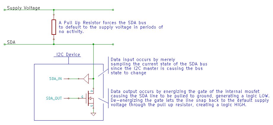
As discussed in the I2C Basics module, the resistors that are commonly seen on I2C circuits sitting between the SCL and SDA lines and the voltage source are called pull up resistors. But what is a pull up resistor?
A pull up resistor is used to provide a default state for a signal line or general purpose input/ouput (GPIO) pin. Typically they are of high resistance thousands or tens of thousands of ohms of resistance. The high resistance ensures that you’re not vampirically sucking too terribly much current on a constant basis through your resistor into your system (5V Vdd / 10000Ω = 0.5mA current), and in fact the Arduino’s main chip, the Atmel ATMEGA328P has internal 20K pull up resistors that can be enabled through code to preset the GPIO pins to a logic high state.
In the case of I2C, the circuitry internal to the SCL and SDA processing subsystems of the chips you’ll use are “open drain”, which means they can sink current, but have no way of sourcing current. That means you supply it to them in the form of the logic high voltage of your circuit, which in the case of the Arduino Uno is typically 5V. In order to establish this high voltage, you attach a pull up resistor between 5V and the SCL and the SDA buses respectively. This is the graphic from the previous module describing that…
However, you can’t just start whacking giant resistors in. There are several things that those resistors interact with that will help to determine what size of a pull up resistor you’ll need.
I2C Logical High and Low
The “Low Input Level Voltage”, rL, is 0.3 x Vdd
the “High Input Level Voltage”, rH, is 0.7 x Vdd
So, when we hook everything up to our Arduino, we need to ensure that our SCL and SDA lines are above 3.5V to register as a logic high signal, and below 1.5V to register as a logic low signal. Everything in between is… well… HIC SVNT DRACONES.
However, you have to achieve a certain amount of voltage, in order to even get the internal mosfet to conduct on your I2C bus, but not so much that we burn out the pin. Think of it like the LED voltage drop. If you have a 1.7V drop across your LED, it won’t light up unless you supply some voltage greater than that, but you have to limit the current to the value specified in the datasheet to keep from destroying it. So if you have an LED with a 1.7V drop and a current rating of 30mA, you find your current limiting resistor by the following method: (5.0V – 1.7V) / .030A = 110Ω resistor.
In the case of our I2C pins, the rating listed in the datasheet is the VOL and the IOL. This is from the Atmel AT30TS750 Temperature Sensor datasheet that we’ll be using in our first I2C component module coming up.
| Symbol | Parameter | Condition | Value |
|---|---|---|---|
| VOL1 | Output Low Voltage | IOL1 = 3mA | 0.4V |
So, in this case the calculation is (5.0V – 0.4V) / .003A = 1533Ω. That represents the lowest possible pullup resistor value, commonly designated RP you can use, because anything less would burn out your I2C pins. The value of the resistor would be larger with a smaller IOL, so the smallest IOL on the bus would determine the minimum RP.
If you were using a 3.3V supply, and your I2C device had a VOL of 0.4V and an IOL of 2.1mA, what would your minimum resistor value be?
I2C Bus Capacitance
A capacitor is a pair of electrically conductive surfaces with some sort of dielectric material sandwiched between them. This is pretty much also the exact definition of what a printed circuit board is. Unless you’re doing home etching or cheap power supply design, your boards will have the capability of copper laid on both sides of the board. Typically, at least one of those sides is used as a “ground plane”, meaning a giant field of copper that can be connected to from any point on the board by drilling a copper plated hole through the thing to provide a very quick and very low resistance path to ground. The thing that gets drilled through, is typically a material called FR4, a form of fiberglass… technically a flame resistant glass-reinforced epoxy laminate sheet if you’d like to impress your geek friends. What you wind up having is copper on the top, copper on the bottom, and dielectric smack dab in the middle: a capacitor — a dramatically inefficient one — but a capacitor none the less.
Each of the SCL and SDA pins in your I2C circuit will also have some form of pin capacitance. Going back to the AT30TS750 datasheet it specifies the pin capacitance here…
| Symbol | Parameter | Min | Max |
|---|---|---|---|
| CI/O | Input/Output Capacitance (SDA and ALERT pins) | VI/O = 0V | 8 pF |
| CIN | Input Capacitance (A2-0 and SCL pins) | VIN = 0V | 6 pF |
So, you’ve got a bunch of little capacitors all laying around connected to your I2C buses, why do you care? Because a capacitors job is to develop and release a charge across it’s conductive elements, and the larger the capacitor, the longer it takes for that charge to build up or release. So if your I2C bus, with all the PCB capacitance and pin capacitance added together, winds up with a capacitance large enough, it will work to prevent the rapid changing of a voltage level on that bus, and suddenly you can’t make those quick snaps from logic low to logic high as cleanly as necessary.
And how does this funky capacitor get charged? From Vcc through your pull up resistors! Your circuit and your pull up resistor form a big RC network (resistor / capacitor not remote control) that governs the charge and discharge rate of your capacitor. Now, mind you, this is a teeny, teeny capacitor. The maximum of all the capacitances are limited to 400pF by I2C standard, and you’d have to have either a really long signal trace on your PCB or a lot of devices on it to get anywhere near 400pF, but as the frequency of your signal increases, the impact of that charging rate will have a dramatic affect.
I know this is outside the lines of digital electronics and in the hazy funk of analog stuff, but we’ll go slow.
Let’s start by figuring out the total bus capacitance of our circuit, the CBUS.
We have our temperature sensor, which we already see above has an SDA CP of 8pF and an SCL CP of 6pF. The Real Time Clock, which we’ll cover later, has a CP of 10pF for both pins. So our SDA CP is 18pF and our SCL CP is 16pF total so far.
Now the tricky part. How in the hell do you measure the capacitance of your PCB’s signal trace!? Well, there is fancy test and measurement equipment you can use to do that, none of which are in my price range. We can model it though. For a simple signal trace on a two layer board with the trace on top and the ground plane on bottom you need to know the trace width, the trace thickness, the trace length, the thickness of your PCB substrate (typically FR4), and the “relative permittivity” of your substrate (a way of stating just how dielectric your dielectric is). Now this all takes a bit of research, but I was able to cobble together the numbers for the I2C and SPI Education Shield, and then used the Missouri University Microstrip Impedance Calculator to determine what my capacitance in pF/inch was.
- I specified the trace width in KiCad when I was doing the design, so I know from my design files that it was .010″.
- The trace thickness I found by looking up the PCB spec from OSH Park, who said that a two sided board uses 1 ounce copper. Using a value I found at PCBUniverse, a 1oz copper plane is 0.00137″ thick.
- The trace length I found, again, in KiCad: 1.1058″ for the SCL net and 1.0130″ for the SDA net.
- The thickness of the FR4 I found, again, at OSH Park: 0.063″.
- The relative permittivity I found by first confirming that the substrate was FR4 on OSH Park, then looking up the value for it on Wikipedia: 4.8.
After you throw all of that data into the Impedance Calculator, you get 1.127 pF/inch for the capacitance of your board, making a copper trace capacitance of 1.127 pf/inch x 1.1058 inches = 1.25pF for the SCL net and 1.127pf/inch x 1.0130 inches = 1.14pF for the SDA net.
Adding the total CP to each of their respective nets yields…
- CBUS for SCL = 17.25pF
- CBUS for SDA = 19.14pF
Here’s all of that in a slightly easier to read table…
| Bus | Trace Width | Trace Thickness | Trace Length | Dielectric Thickness | Relative Permittivity | CBUS |
|---|---|---|---|---|---|---|
| SCL | 0.01000 in | 0.00137 in | 1.10580 in | 0.06300 in | 4.8 | 17.25 pF |
| SDA | 0.01000 in | 0.00137 in | 1.01300 in | 0.06300 in | 4.8 | 19.14 pF |
Ok, great. Now what the hell do you do with it? Remember, our concern is determining the highest value of resistor that still allows the SCL and SDA signals to snap between the low and high states in sufficient time, without getting all laggy and curved because of excess charging time.
There is a formula, derived from the RC time constant, that brings all of this together (see section 7.1 of the I2C Manual for the algebra involved). It looks like this…
\[R_{P(max)} = \frac{t_{r}}{0.8473\cdot{C_{BUS}}}\]
The value of tR is the maximum allowable rise time of the I2C signal. If you think about it without all the numbers… the larger the resistor, the longer it takes for the capacitor that is your circuit to charge, the longer it takes from the signal to rise to a logic high. The faster you need to rise, meaning the speed at which you’re running your I2C circuit, the smaller the tR becomes. The value of tR for the common I2C modes are as follows…
| I2C Mode Name | I2C Speed | Rise Time Value tR |
|---|---|---|
| Standard Mode | 100kHz | 1000nS |
| Fast Mode | 400kHz | 300nS |
| Ultra Fast Mode | 1000kHz | 120nS |
We have all the parts we need to determine our maximum RP. Let’s choose the 400kHz Fast Mode and use the values we found for the Education Shield. Remember that all our values displayed so far have been listed in nice big “nanoseconds” and “picofarads” so we have to adjust the nanoseconds to seconds (x 10-9) and picofarads to farads (x 10-12).
\[SCL R_{P(max)} = \frac{300nS \times 10^{-9}}{0.8473\cdot{17.25pF \times 10^{-12}}} = 20525.56\Omega \]
\[SDA R_{P(max)} = \frac{300nS \times 10^{-9}}{0.8473\cdot{19.14pF \times 10^{-12}}} = 18498.74\Omega \]
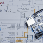
An 18K resistor represents the largest resistor we could use for pullup resistors on the I2C and SPI Education Shield (because 18K would work for both buses, no need to use two different values). Conversely, a 1K5 resistor is the smallest value we could use without burning up the I2C pins of our devices. We want to hit a value somewhere in the middle, and that is why when you look at the schematic excerpt of the I2C subsystem from the Education Shield at the very top of page, the pull up resistors are 10K.
These two aspects of pull up resistor specification are captured in these two charts from the NXP I2C Manual (note: the Arduino is not capable of Fast-mode Plus)…
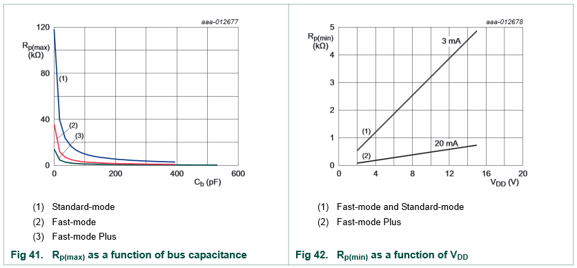
CBUS Greater Than 200pF
In the event that you have a bus capacitance that exceeds 200pF and you are attempting to drive the I2C bus at Fast Mode speed or greater, pull up resistors will no longer be sufficient, and you’ll need to investigate the use of a current source or switched resistor circuit to supply the SDA and SCL logic high voltage necessary to achieve those signalling speeds with that much CBUS.
I2C Pull Up Resistor Bottom Line
If you’re working with a single chip on a breadboard, just use whatever resistor value you have on hand from 4K7 to 10K for your SDA and SCL signals and you’ll be fine. Going through all the calculations above only becomes critical when you begin laying out your own PCBs and start loading more than one or two I2C devices into your circuit. You can see that the difference of 1.89pF between the SCL and the SDA buses above lowered the allowable resistance by over 2000Ω. Consequently, long PCB traces (or even worse using a ribbon cable to attach a device to the bus) or adding multiple devices with their pin capacitance will have a very significant effect on your RP value.