Let’s put all this stuff together and actually build a couple digital logic projects! Truth be told, I’m not about to present a single thing that isn’t waaaaaayyy easier to accomplish with a few lines of code and your devboard of choice, but building things this way will at least give you an appreciation for just how astonishingly nimble your ATTiny is.
Digital Logic Circuit Guidelines
I want to provide some quick rules for building real world practical digital logic circuits. To this point, we’ve only been building individual discrete chunks of logic — gates and flip flops. Now that we’re going to start combining them into stuff, I need to be a little more grown up about things I’ve been totally ignoring to this point.
Supplying Power
You’ve seen this splashed across all the Digital Logic pages so far…
Let that be a reminder that you do, actually, need to provide power and ground to your chips to make them dance.
TTL vs CMOS
If you have a selection of chips to choose from to build this stuff, you need to make sure that you are using chips from the same “family”. In part one I briefly mention the difference between TTL and CMOS chips, and now it’s vital that you know which is which. The two cannot be used interchangeably without building interfaces between them, which is an unnecessary hassle for the most part — just use all CMOS or all TTL. If you’re not sure if you’re using TTL or CMOS, check the datasheet. Here is an example of the difference between the two…
| Rating | SN7402 | SN74HC02 |
|---|---|---|
| Min Input Voltage | 4.75V | 2.00V |
| Max Input Voltage | 5.25V | 6.00V |
| Min. High Level | 2.00V | Vcc = 2.00 / High Level = 1.50V |
| Vcc = 4.50 / High Level = 3.15V | ||
| Vcc = 6.00 / High Level = 4.20V | ||
| Max. Low Level | 0.80V | Vcc = 2.00 / Low Level = 0.50V |
| Vcc = 4.50 / Low Level = 1.35V | ||
| Vcc = 6.00 / Low Level = 1.80V | ||
| Switching Speed | 12-22ns | 6-13nS |
| Datasheet | SN7402 | SN74HC02 |
Power Supply Decoupling
The more switching of signals you do in your circuit, the more noise your going to create on the power rails. Make sure that you add a bypass capacitor as close to the Vcc pin of your logic chip as possible to prevent the noise from entering the chip. There is more information on this in my article on Bypass Capacitors.
Logic Level Switching
“Logic Level” means that you don’t want to apply voltages to these things that are either higher than Vcc or lower than ground. Anywhere. If you need to control a signal outside those limits by means of logic levels, put a transistor or a mosfet in there and manage that.
Complete Hookups
Don’t leave unused inputs floating. It’s bad form, and introduces more noise into the system. Connect them to Vcc so that they are in a defined state.
Buffered Power Supply
Depending on how many of these chips you’re connecting, what they’re outputting and how much they’re switching, it might be a wise idea to place a 10uF capacitor across the power rails to both manage a little bit of noise, and act as a “reserve tank” of electrons.
Digital Logic Project 01: Debounced Switch
- 1x DPDT Switch
- 1x SN74HC04 or equivalent NOT
- LEDs and resistors for output if desired
Let’s start with something nice and simple, straight out of the Forrest Mims, “Electronic Formulas, Symbols and Circuits“. This is from page 150.
There are several ways to debounce a switch: microcontroller code, RC networks (which I used for the I2C and SPI Education Shield) but here we’re going to use a set of NOT gates.
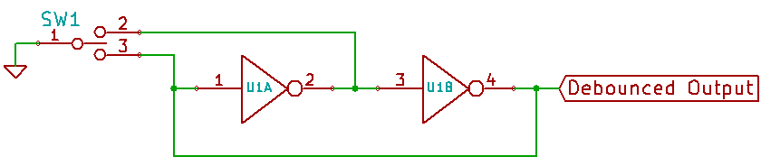
Essentially, you connect your DPDT switch, such as the one we’ve been using all along to control our various logic models, to a NOT gate and use it to control the output of the NOT gate, rather than using your switch to control the circuit. In this method, you’re letting the NOT gate swallow up the bounces within its propagation delay and output a nice clean signal. The output is used as feedback into the system enforcing the high or low level. When the switch pulls the bottom contact (3) to ground, it brings the input on the first inverter low, which make’s it’s output high, making the output on the second inverter low, hence, low output with a low feedback. When the top contact (2) of the switch is brought to ground, you make the input on the second inverter low, making it’s output high, hence, high output with a high feedback. Here’s the truth table…
| SW2 | SW3 | NOT 1A | NOT 1Y | NOT 2A | NOT 2Y | OUTPUT |
|---|---|---|---|---|---|---|
| LOW | HIGH | LOW | HIGH | HIGH | LOW | LOW |
| HIGH | LOW | HIGH | LOW | LOW | HIGH | HIGH |
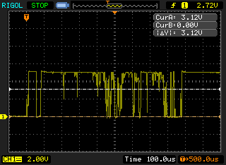
Undebounced Switch Signal
You may be curious what the actual effect is on the switch. Well, here is the output of the switch when I connected it to my scope. I’ve moved the signal down the Y axis a bit so you can see the whole shebang. The white cursor line is set again to 3.12V, which is the HIGH threshold listed in the datasheet. Not that you really need to see it there because that signal is so bad it looks like a tattered bead curtain from the 70s. And mind you, we’re in a time domain of 100µS. The rise/fall time of the logic we’ve been working with is in the nanoseconds, so if you tried to use this as a clock signal, you’ve just registered, by my scientific reckoning, a metric shit ton of clock pulses in the span of 900µS.
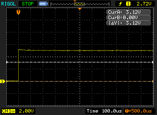
Debounced Switch Signal
Compare that now against the smooth jazz of our switch, debounced with a pair of not gates. That’s a brickwall of 5V goodness right there. Again, the white cursor is at 3.12V, and, again, it’s unnecessary because that signal just doesn’t bounce at all. It’s tremendously clean. You could easily use this as the clock pulse to control any of the circuits we’ve been building so far. The question is, just how clean is that signal?
ENHANCE (pay attention to the time scale in the lower right hand corner)
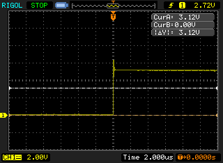
2.000µs per division
At 2.000µS it still looks pretty vertical, although there’s a rough spot up at the top where we may be seeing some affects of oscillation.
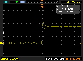
200ns per division
At 200ns, the roughness at the top of the signal is starting to resolve itself, showing that the NOT gates aren’t absolutely perfect. The question is, does the signal ever dip below the white line designating 3.15V, our mandatory minimum voltage we have to be at or above in order to qualify as a defined logic high.
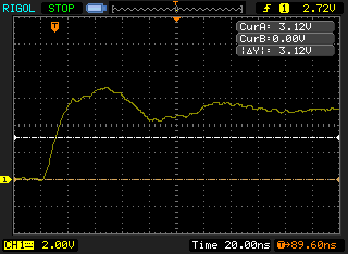
20ns per division
At 20ns, the oscillation of the switch bouncing is shown in the highest resolution I can squeeze out of my scope. Obviously some remnant of the original switch bouncing is still present, but it’s being managed well above the 3.15V threshold. There is a single, clean transition from 0V to >3.15V on the left, and even though it’s not entirely smooth for the first 160ns or so, it eventually levels out.
Right down to 20ns, the signal still rises and stays above the 3.12V threshold. It’s a little lump, but lumpy is ok, spiky is bad.
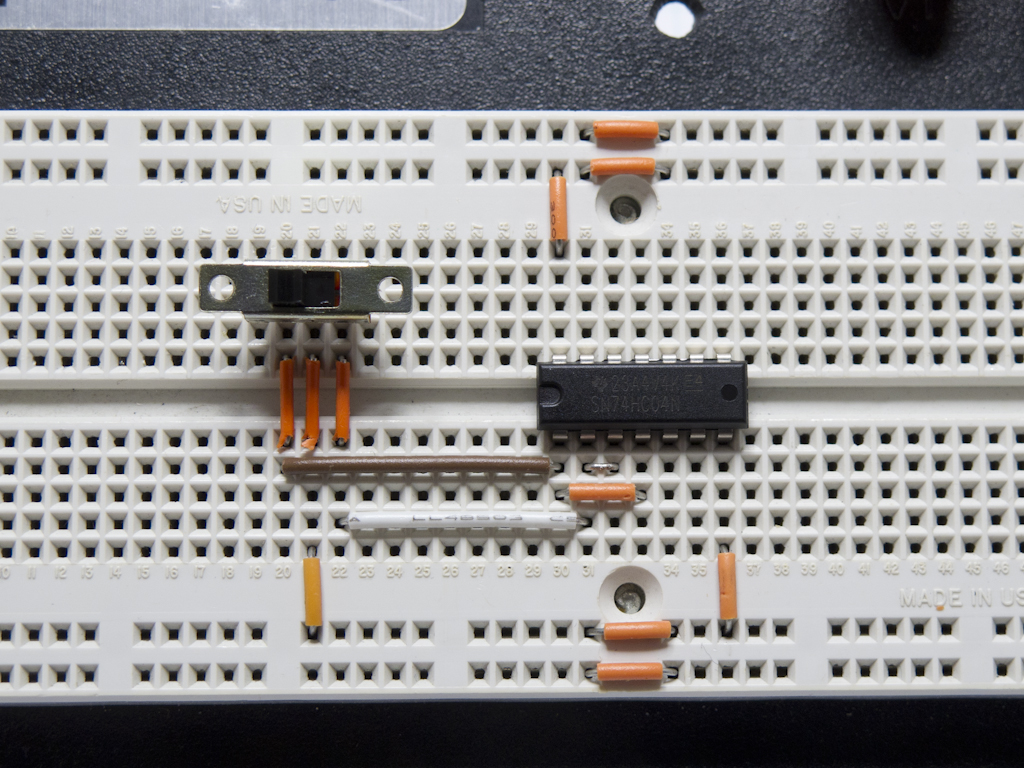
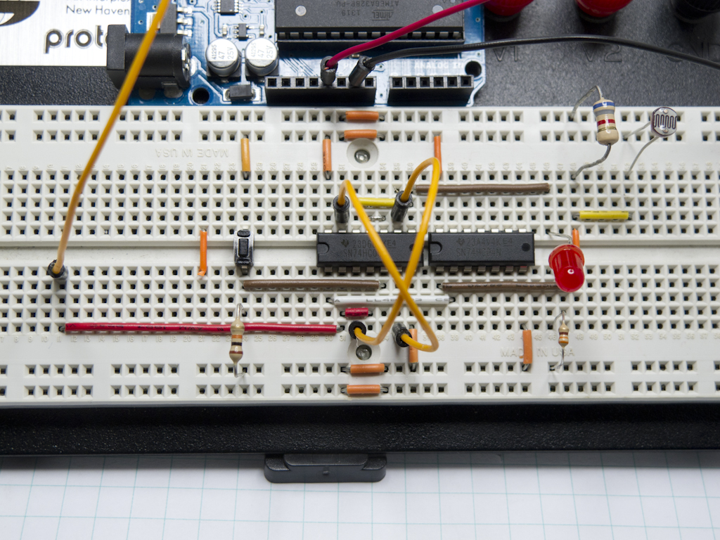
Here is the circuit built out on a breadboard. Hopefully the traces above will serve as better examples than me hooking this up to an LED or something.
If you don’t have an oscilloscope but want to see a before and after example of switch debouncing, build an edge triggered SR flip flop, and instead of using a signal generator for your clock, use a tactile button and see what happens, then incorporate the debounce circuitry.
- 2x tactile buttons
- 2x 10K pull down resistors
- 1x 74HC04 or equivalent NOT
- 1x 74HC00 or equivalent NAND
- LEDs and resistors for output if desired
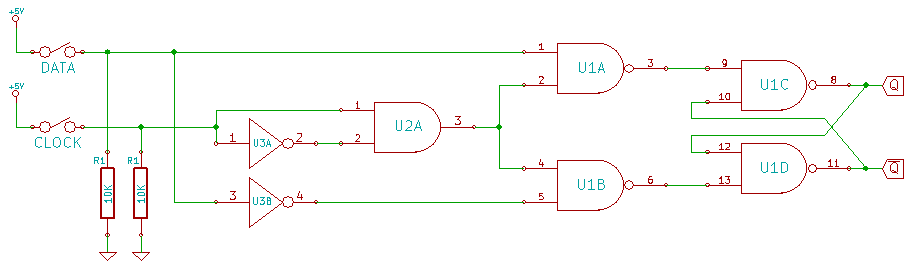
That’s the schematic for the undebounced circuit. You can use LEDs with resistors for Q and NOT-Q. It will be good practice to figure out how to integrate the two schematics yourself to create the debounced circuit. Fortunately, the 74HC04 has six inverters on it.
Digital Logic Project 02: Clocked SR Flip Flop Light Detector
- 1x clock signal generator
- 1x tactile button as reset
- 1x 10K pull down resistor
- 1x Light Dependent Resistor
- 1x 6K8 resistor
- 1x 74HC04 or equivalent NOT
- 1x 74HC00 or equivalent NAND
- LED and 330 resistor for output
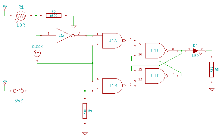
In a previous part of the Digital Logic Basics, I talked about having the kitchen light know when it needs to turn on and do so by itself. Here’s a little light detector circuit I just threw together. The flip flop is a clocked, level triggered SR flip flop. The light detector is going to use a light dependent resistor, but think of it as a stand in for any kind of sensor. If it’s a digital sensor, great, you’re already in the HIGH/LOW signalling ballpark. If it’s an analog output as the LDR, you can use a voltage divider to bring the sensors output inline with your needs, as we do here.
On the SET input, a light dependent resistor forms a voltage divider with a fixed resistor, calculated so that when the LDR is exposed to the fluorescent lights in my office, the voltage level remains above 3.15V, the threshold for a high input signal. When it’s in shade, the voltage will drop below 1.35V, the threshold for a low input signal. When it brightens up again, the voltage level will rise to a high state again. This signal is sent into an inverter so that when the lights are on, it provides SET with a low.
On the RESET input, I have a 10K pull down resistor so that it is lightly pulled to GND. I’ve also included a simple SPST tactile button, so that you can momentarily bring RESET high to clear the light detection. You don’t need to worry about debouncing this.
For CLOCK, I have an Arduino pulsing a 50Hz frequency signal with a 50% duty cycle (50Hz = .020 second period, 50% duty cycle = .010 seconds high, .010 seconds low). I wanted it relatively fast so that you weren’t sitting there trying to guess when the clock was high or low to reset. The Arduino isn’t necessary, any clock generator in that same range should do, like a 555 Timer.
For the output, just a simple LED with a current limiting resistor taking the place of whatever else you might want to put there.
Here’s how it works: when the lights are on, the indicator LED is off (the system is in RESET, because the inverter is keeping SET low). When it goes dark for the LDR, the voltage drops, causing the inverted output to go high, placing the flip flop into SET and the LED goes on. It stays on too, even after the lights come back up, because even though the voltage at the SET input drops again, it just enters the HOLD state. Then after you do what you have to do because you detected the signal (reprimand your hamster, or whatever) you press the button to reset the system.
Be aware, this is just a simple SR flip flop, not a D-type and not a JK type, so there is the risk of the INDETERMINATE, meaning you would push the button while it’s dark: high SET and high RESET.
Digital Logic Projects 03: Learning Why You Buy Integrated Circuits
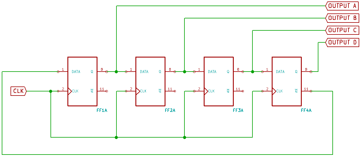
The circuit shown is a 4-bit counter, comprised of d-type flip flops connected in series, with DATA connected to Q over and over, until you get to the last one, where NOT-Q is connected back to the first DATA. Each time the clock pulses, in increments the high state across the outputs in sequence. This allows you to use a single clock and achieve a cascaded output over many stages. In this case I was going to try to build a four stage counter, because that’s how many DIP packages of NAND gates I have.
So I started building it, and when I started running out of jumper wire I realized I was just wasting time. Above a certain level, it serves no purpose building circuits out of individual logic gates unless you’re in high school and have nothing but time on your hands in the summer, or programming an FPGA.
You actually need 16 NAND gates to build the four flip flops, a NOT gate for every data input (to connect SET with RESET) with NOT and AND gates to create a positive edge triggered clock inputs. Then you need jumper wire to hook it all up… and then you realize that you can just buy this already assembled in various IC forms. This is what the beast was looking like before I stopped…
As an example, you know inside and out by now what a D-type Flip Flop is. The CD4013B is a pair of them in one chip. If you want to get really crazy, the SN74HC574 accepts a single clock signal, with eight data inputs and eight Q outputs. Up above, there’s the schematic for a four bit counter, well, here’s the CD40192B that counts up, counts down and includes PRESET, CLEAR and the ability to daisy chain. Any of those cost about $0.50 each.
Jumper wire costs more.
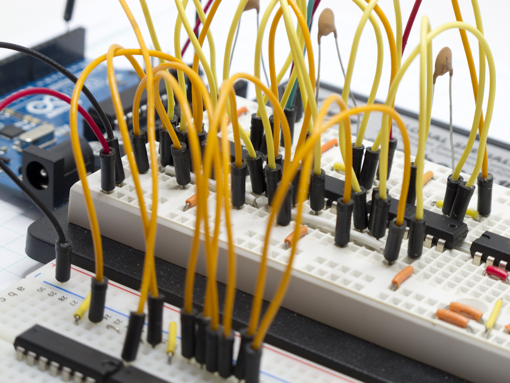
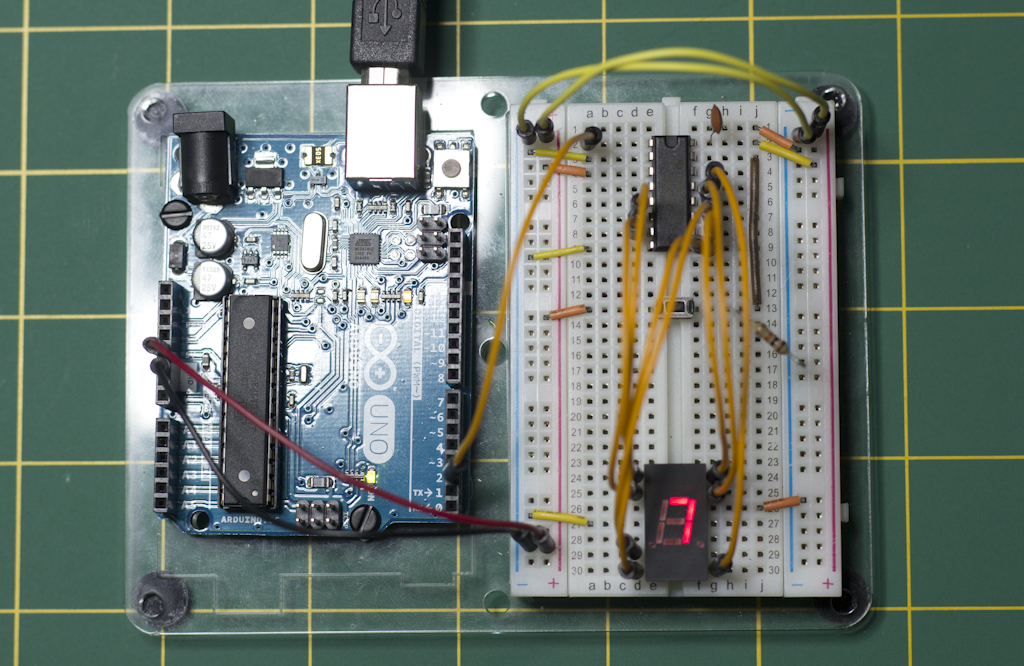
Digital Logic Projects 04: CD4026B Decade Counter with Seven Segment Output
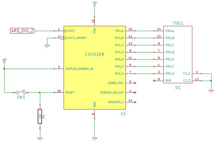
Rather than try and build it out of discrete components like above, we’re now using an integrated circuit to do the job for us. The CD4026B is a “decade counter” (counts up to 10) but instead of just delivering a 10 Q pin out, it encodes the value internally to a number for display on a seven segment display. In this case, we’re sourcing the current for the display, so it needs to have common cathodes.
Each time the clock signal goes high, it increments the counter, 0-9, then starts over. It features the ability to carry the value to a subsequent counter too, but we’re only using one chip and one display for this project.
If you couple this with the LDR from above, you could get a count of how many times the light was dimmed instead of just a binary “was it dimmed or not”.
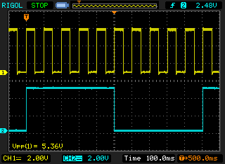
Decade Counter Carry
The CARRY OUT feature of the chip allows you to add tens places to your count by clocking out a high signal for every 10 high signals in. In the oscilloscope capture to the left, you see the yellow trace showing 10 ticks of the clock, but the blue trace, showing the carry, clocks out the same period x10. In this case, the clock is on a 100ms period, so the carry is on a 1s period.
Fortunately, the Texas Instruments datasheet for the CD4026B actually shows the full breakout of the internal logic for the chip. If you’ve followed through all the way from logic gates through flip flops, to clock and data signals, then patterns in this schematic should start looking like they make sense.
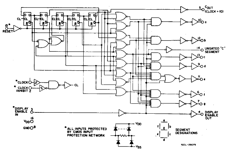
If you look in there, you’ll see Pin 14, UNGATED “C” SEGMENT. I’ll leave it up to you to play around and figure out why it does what it does, and how you can use it. Here’s the oscilloscope trace for it’s timing…

Further Reading
Practical Electronics for Inventors by Paul Scherz. I highly recommend the digital logic section in that book as it was the resource that finally solidified all the gates for me and how they were put together to make flip flops, etc, etc. It’s no flaw that the progression on Digital Logic Basics Parts 1 – 5 of this site follow the progression of knowledge in that book, although hopefully I help to flesh the details out with actual measurements, schematics and builds. I have the first edition that I bought in 2000 and it’s up to the third edition now. If you can find a copy of it used, the digital logic section hasn’t changed.
Electronic Formulas, Symbols & Circuits by Forrest Mims. If you don’t have a copy of all of his Engineer’s Mini Notebooks by now, I don’t know what you’re waiting for. Go by them. All of them.
Paul Falstad’s Circuit Simulator There is an entire section of simulators for Combinational Logic and Sequential Logic.