In the first part, Digital Logic Basics Part B01, I covered the various forms of digital logic gates, hooked them up and measured them. Now we’re going to move from the individual gates to learning how they are combined to form something called a “flip-flop”.
Previously, I made the analogy that you could use digital logic to store a state of something, like turning on a switch and having the kitchen light remain on, except that isn’t entirely correct. The light switch analogy exhibits a quality like the logic circuits we put together in the first part: you apply an input signal and get some form of output. Great. However, you need to maintain that signal or the output will change. Ideally, you’d like to be able to pulse your desired inputs to set your output, then forget about it.
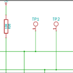
We can chart out the actual functioning of the kitchen light by using a diagram like this…
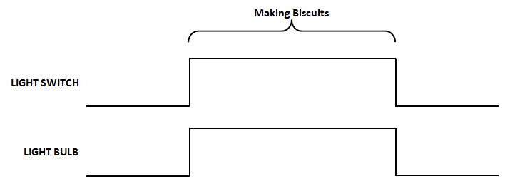
That tells us quite a few things. First, the light is dependent on the switch. Second, when the light switch goes high, the light bulb goes high. Third, when the light switch goes low, the light bulb goes low.
Now, let’s compare this with a living room light. This is the kind of light that you plugged into the wall to make it convenient to turn on and off, but also has one of those rotary switches directly on the cord, that your significant other uses to turn it on and off when they’re reading. So, it’s late at night, you’ve just come home from work, you want to sit on the couch so you flip the living room wall switch on and nothing happens. You curse silently as you stub your toe into the coffee table, knock over the half finished mug of coffee on the end table while fumbling for the cord switch and once you turn that on, the bulb goes on. But if you flip either of the two switches off, the light will go back out. Here’s the diagram for this scenario:
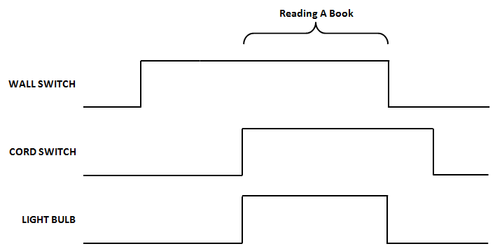
What you’re looking at there, is an AND gate. The wall switch is input A, the cord switch is input B and the light bulb is output Y. The light turning on is direct reflection of the input switches: you must create the AB state in order for Y to go high. How can we modify this so that we can set the state or reset the state by rapidly switching the inputs, but have the state maintained after the inputs go low again?
The answer is a flip-flop.
SR Flip Flop
We need to move away from “A”, “B”, “ON, “OFF” and other terms that regular humans might understand, and move into some more engineering-ish nomenclature.
- SET – abbreviated “S”. One flip-flop input.
- RESET – abbreviated “R”. The other flip-flop input.
- Active Low – the opposite of how you normally think of things… considered active when the signal is in the low state. This is commonly denoted by using an overbar over the signal as you will see with “NOT-Q” below.
- Q – One output of the flip-flop. When Q is high, we consider the flip-flop to be in the SET state.
- Q – The other output of the flip-flop, called “NOT-Q“. (I’m going to refer to it this way constantly, because the actual HTML to generate a Q with an overbar is kind of a pain to type out.) When NOT-Q is low, the flip-flop is considered to be in the RESET state.
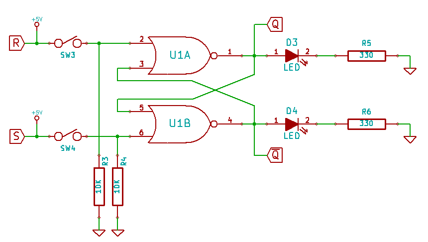
In part one, I showed how you can combine NOR gates to create an XOR gate, and in this case, we’re going to combine NOR gates to create a Set-Reset Flip Flop (SR Flip-Flop).
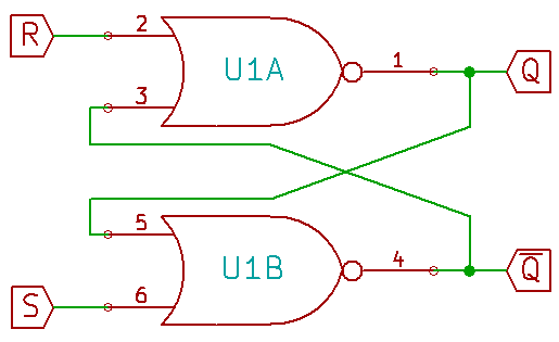
If you’re like me, then you’re probably looking at that diagram and thinking, “Nice picture, but why is that so significant?”. The important thing is that the outputs, Q and NOT-Q, are tied to the inputs! You’re providing feedback into the system.
Let’s go to the truth table, Marv.
| S | R | Q | NOT-Q | Flip-Flop State |
|---|---|---|---|---|
| LOW | LOW | UNCHANGED (Q) | UNCHANGED (NOT-Q) | HOLD |
| LOW | HIGH | LOW | HIGH | RESET |
| HIGH | LOW | HIGH | LOW | SET |
| HIGH | HIGH | LOW | HIGH | INDETERMINATE |
Flip Flop States
So this is a little tricky. We have two states that seem clear, “SET and “RESET“, but what the hell are HOLD and INDETERMINATE? More importantly, how can you determine what the outputs are, if the output REQUIRES the output itself to determine output state? Circular logic witchcraft!
1. SET State
Let’s start out by reviewing what a NOR gate does. Here’s the truth table as a quick reminder…
| Input A | Input B | A NOR B |
|---|---|---|
| LOW | LOW | HIGH |
| LOW | HIGH | LOW |
| HIGH | LOW | LOW |
| HIGH | HIGH | LOW |
It only allows a high state, when both inputs are low. So if we bring SET high, we know that NOT-Q will be forced low. If NOT-Q is low and RESET is low as well, then Q is high :: SET = HIGH = SET STATE</span.
[masterslider id=30]
2. RESET State
This works in the opposite way as well, if RESET is high, Q will be forced low and since Q is low and SET is low as well, then NOT-Q is high :: RESET = HIGH = RESET STATE.
[masterslider id=31]
3. HOLD State
Let’s take that RESET condition and bring RESET low again. What happens? SET is already low and as you bring RESET low nothing changes: NOT-Q is still high because of the simultaneous LOWs on it’s inputs… Since Q is forced low and SET is low, then NOT-Q remains high. The circuit is holding the output state! (If you do the logic starting with a SET condition, bringing the inputs low results in holding the SET condition as well.) It doesn’t make for the most interesting slideshow, but in the interests of thoroughness.
[masterslider id=32]
4. Indeterminate State
What’s with the indeterminate state? Well, the problem isn’t so much with the functioning of the NOR SR flip-flop when both SET and RESET are high, it’s clear that in this instance, both outputs would be low, period, although I can’t fathom why you would ever need to be in a SET and RESET condition simultaneously. You run into an issue when you attempt to go back into the HOLD state from this. As soon as one of those inputs goes low, it’s going to flip the output high… but which one? We’re talking on the nano-second scale here. In the real world, there’s simply no way to tell whether SET or RESET is going to go low first, so you cannot predict the outcome from this scenario: the state cannot be determined because the SET and RESET inputs are racing each other to the low state, which is why this is also called a “race condition.”
The way to get around the indeterminate state then, is to preset a valid condition first, either SET or RESET, then simply prevent the indeterminate state from occurring through your design.
Building and Testing a NOR SR Flip Flop
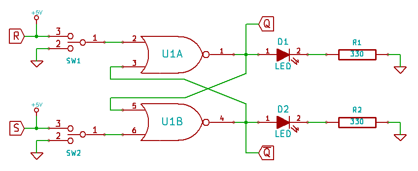
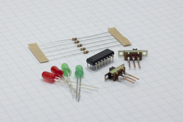
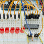
With this circuit, we’re taking the SR Flip Flop from above and adding some LEDs on the output, and some Single Pole Double Throw switches to control our SET and RESET signals. The R, S, Q and NOT-Q flags in the schematic are just there to illustrate which signal is which, not as signal pathways. In addition, I have added some green LEDs to my circuit so that it’s very obvious to the camera when the SET or the RESET switch goes high, they’re not on the schematic though, because they aren’t really necessary other than for the photographs.
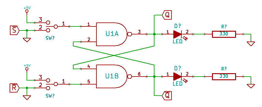
You can also easily use some standard tactile buttons on here, I just needed to use the slide switches so I could show the inputs energized in the pictures. Here is a schematic showing how to hook up the tactile buttons. If you do use a tactile button, make sure that you connect a 10K resistor between the SET pin and GND and the RESET pin and GND. That establishes a defined state for those pins, but won’t dump a ton of current (.5mA) when you bring the pin high. Without the pull down resistors, when the button was open, you’d be leaving the inputs floating and get indeterminate outputs.The chips we are using have four to six logic gates on them. If this were a full working circuit that was going to be doing some rapid switching, you would absolutely need to tie the inputs of all the other gates in the chip to Vcc, so that they aren’t left floating. Before we do anything else with the circuit, go ahead and take the jumper wire that’s providing your 5V power rail, and just stab it in and take it out a couple of times. What you should see is the LEDs turning on randomly. That’s because we’re energizing the chip in an indeterminate state. In order to begin using it, you must establish a valid state, either SET or RESET. I chose RESET.
With a valid state created, you then energize one input, either SET or RESET, and then return it to GND. When you change from one state to the other, you will see the corresponding LED light up and then hold in that state when you GND the inputs.
[masterslider id=33]
Pretty cool eh?
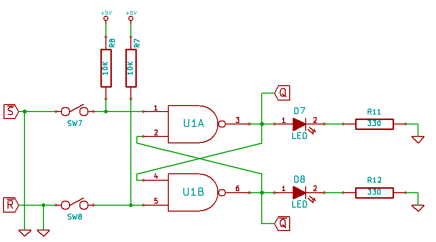
Building and Testing a NAND SR Flip Flop
In none of the schematics do I show Vcc or GND being connected to the logic gates. I did that to make the schematics as clear to understand as possible. Any of the logic gate ICs you use in your circuits will need to have pin 7 connected to GND and pin 14 connected to Vcc.
Turns out you can build these out of NAND gates too. There is a vital difference though: in the case of a NAND gate, the inputs are active low.
Both schematics are offered: the one using SPDT switches shown above and one using tactile buttons. There are a lot of things different between this and the NOR based flip flop above. Firstly, the pin out between the 74HC00 and the 74HC02 are different ABY vs. YAB. Second, the SET and RESET signals are swapped top to bottom and as they are active low, they are now NOT-SET and NOT-RESET. As a result, pay careful attention to which signal you’re sending to the NAND flip-flop. Finally, the most crucial change to note is the indeterminate state is now comprised of two low signals, the exact opposite of the above. That means the HOLD state is generated when both signals are high.
As before, a quick review of the truth table…
| Input A | Input B | A NOR B |
|---|---|---|
| LOW | LOW | HIGH |
| LOW | HIGH | HIGH |
| HIGH | LOW | HIGH |
| HIGH | HIGH | LOW |
1. SET State
A NAND gate goes low only when both inputs are high (the opposite of our living room light scenario). So to put it in the SET state, we bring the NOT-SET pin low, which forces Q high. Since Q is high and NOT-RESET is high, NOT-Q is low :: NOT-SET = LOW = SET STATE.
2. RESET State
If we bring NOT-RESET low, that drives NOT-Q high. Since NOT-Q is high and NOT-SET is high, Q is low. NOT-RESET = LOW = RESET STATE.
3. HOLD State
Remaining in the RESET condition, if we bring NOT-RESET back high, NOT-Q remains high because of NAND logic.
4. INDETERMINATE State
While the state of the indeterminate input is the opposite of what it was for the NOR gate flip flop, the end result is the same: a race condition.
Confused yet? Trust me, once you’ve put these circuits together a couple of times, you’ll get the gist of it. Particularly if you’re like me and screw up the pin out connection every. single. time. It might be helpful to also print out a copy of the schematic and mark out little “+” and “-” on it in pencil to diagram out each logic state.
Here is the NAND SR Flip Flop in action…
[masterslider id=34]
So now you have a way of working with a signal that goes low when something changes (use a NAND flip flop) or goes high when something changes (NOR flip flop).
Timing Diagrams
So remember the charts up above where we looked at how the different states interacted for the kitchen light and the living room light? Those are your introduction into the world of timing diagrams.
Timing diagrams illustrate, or at least attempt to illustrate, what occurs when various digital signals are in their respective states. It’s called a “timing” diagram because usually you’re using a clock signal as a reference, but we haven’t looked at clock lines yet (soon!).
Take, for example, our NOR based SR Flip Flop above…
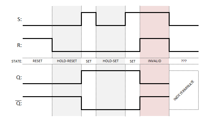
Moving left to right, we first begin in a RESET state. The RESET pin is brought low, leaving us in HOLD–RESET. The SET pin is brought high and we enter the SET state. SET is brought low and we enter the HOLD–SET state. SET is brought high again, which puts us technically into a SET state although it doesn’t affect the outputs. Now the RESET is brought high as well, putting us on the path to the indeterminate state.
For the sake of thoroughness, and because we’re going to be using the NAND flip flop for other things in part 3…
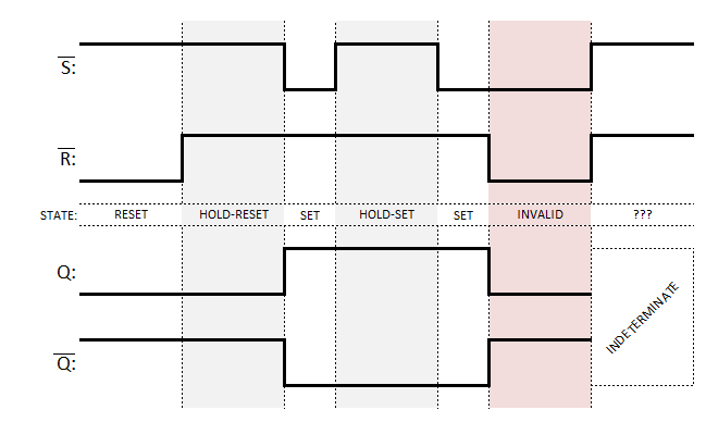
Moving again left to right, we begin in the RESET state. The RESET is brought high, leaving us in HOLD–RESET. The SET is brought low and we enter the SET state. SET is brought high and we enter the HOLD–SET state. SET is brought low again, which puts us technically into a SET state, although it doesn’t affect the outputs. Now the RESET is brought low as well, putting us on the path to the indeterminate state.
As you move into doing more serial communication you’ll wind up studying timing diagrams in detail, understanding how many bits are being sent on clock signals and at what point something MUST go high/low to make something happen. It’s a big puzzle.
Sometimes, those puzzle pieces are good…
Sometimes, those puzzle pieces are the technical equivalent of the Faerie’s Aire and Death Waltz…
In our next exciting episode, we’ll look at synchronizing all of this with a clock signal and learn about level vs. edge triggering!
