I’ve taken a lot of notes on shift registers, configuring them this way and that, and actually incorporating a manually functioning one into the I2C and SPI Education Shield. As I did more research into how they worked, I kept running across phrases like “a shift register is a cascade of flip flops, sharing the same clock, in which the output of each flip-flop is connected to the ‘data’ input of the next flip-flop in the chain’ (Wikipedia). What does that actually mean? Why are some chips positive-edge triggered and some negative? What the hell is a “latch” anyway?? I never went to university, where I assume this subject is covered in quite some depth, so it was important for me to take this down to it’s basic principles. It’s a habit of mine — I don’t like “just making it work” — I want to know why it works the way it does. So, if a shift register is made of flip-flops, what are flip-flops made of? The answer is: digital logic.
Digital Logic Defined
Both parts of that phrase, “digital logic” are incredibly, some (me) might say sublimely, simple. By “digital” we mean a system of discrete values (analog being a magical mix of fluctuating funk), the most basic values being “YES” and “NO” otherwise noted as “1” and “0” and for our purposes as “some specific voltage” and GND. By “logic” we mean the way these values act when combined under very specific rules such as “AND” or “OR” among others. That sentence itself contains logic right at the end… what are the specific rules that apply to that those values: AND, OR. Other rules such as “Stepping in front of moving buses is a bad idea”, despite being perfectly valid in their own system, do not apply.
Let’s define some values…
The digital values you’ll encounter most frequently, particularly if you’re just starting out, will be +5V and GND, representing 1 and 0, HIGH and LOW, ON and OFF, TRUE and FALSE, etc. +3.3V (commonly shortened to 3V3) is also very common and there are a mix of smaller values as well. We’re going to focus on +5V for our purposes though.
Our logic rules are going to be NOT, AND, NAND, OR, NOR, XOR and XNOR. Given a set of inputs, those rules will govern what the output is, and we can see this by using something called a “Truth Table”, meaning a table that will explain how those values combine within that rule. As we’ll end up using these for circuits, we’ll talk voltage levels as either high or low.
There are many ways of describing logic states: “1/0”, “TRUE/FALSE”, “HIGH/LOW”, “A/A” (pronounced “A / Not A”). When you see a pin out showing an active-low signal, something like “Output Enable” listed as “OE“, this is where that comes from: the pin is active when it is brought to digital low. You should also note that when you’re looking at the schematic symbols below, the little bubble on the outputs means “inverting”, meaning that pin has the opposite polarity of what it would be.
1. NOT – output is the opposite of the input.
|
INPUT A
|
NOT A
|
NOT SCHEMATIC SYMBOL
|
|---|---|---|
| LOW | HIGH | |
| HIGH | LOW |
2. AND – only results in a high voltage state if all inputs are also high.
|
INPUT A
|
INPUT B
|
A AND B
|
AND SCHEMATIC SYMBOL
|
|---|---|---|---|
| LOW | LOW | LOW | |
| LOW | HIGH | LOW | |
| HIGH | LOW | LOW | |
| HIGH | HIGH | HIGH |
3. NAND – “Not AND” will return a low voltage state only when both inputs are high. You can also think of it as the inverted output of an AND gate.
|
INPUT A
|
INPUT B
|
A NAND B
|
NAND SCHEMATIC SYMBOL
|
|---|---|---|---|
| LOW | LOW | HIGH | |
| LOW | HIGH | HIGH | |
| HIGH | LOW | HIGH | |
| HIGH | HIGH | LOW |
4. OR – results in a high voltage state when one or both of the inputs are in a high state as well.
|
INPUT A
|
INPUT B
|
A OR B
|
OR SCHEMATIC SYMBOL
|
|---|---|---|---|
| LOW | LOW | LOW | |
| LOW | HIGH | HIGH | |
| HIGH | LOW | HIGH | |
| HIGH | HIGH | HIGH |
5. NOR – “Not OR” results in a high voltage state only when both of the inputs are low. Like a NAND gate has the inverted output of an AND gate, the NOR gate has the inverted output of an OR gate.
|
INPUT A
|
INPUT B
|
A NOR B
|
NOR SCHEMATIC SYMBOL
|
|---|---|---|---|
| LOW | LOW | HIGH | |
| LOW | HIGH | LOW | |
| HIGH | LOW | LOW | |
| HIGH | HIGH | LOW |
6. XOR – “Exclusive OR” will give a high output when one, and exclusively one of the inputs is high. When the inputs are matched at either state, the output is low.
|
INPUT A
|
INPUT B
|
A XOR B
|
XOR SCHEMATIC SYMBOL
|
|---|---|---|---|
| LOW | LOW | LOW | |
| LOW | HIGH | HIGH | |
| HIGH | LOW | HIGH | |
| HIGH | HIGH | LOW |
7. XNOR – “Exclusive NOR” will give a high output exclusively both inputs are in a matched state, otherwise the output is low. You guessed it, it’s the inverted output of the XOR gate.
|
INPUT A
|
INPUT B
|
A XNOR B
|
XNOR SCHEMATIC SYMBOL
|
|---|---|---|---|
| LOW | LOW | HIGH | |
| LOW | HIGH | LOW | |
| HIGH | LOW | LOW | |
| HIGH | HIGH | HIGH |
That’s all fantastic stuff, Dan, but why should I give a damn?
Well, assuming you’re reading this because you have an interest in electronics to begin with, the digital logic gates listed above are the fundamental building blocks that allow a designer to alter the state of a signal. Far more importantly though, they allow you to SAMPLE and HOLD that signal state as long as you wish — flipping the switch to turn on the kitchen lights is great, but having the switch maintain that position while you’re making biscuits is vital, and it would be even better if the kitchen lights were able to regularly check the light level in the room and then turn themselves on when it gets too dark.
What Do Digital Logic Gates Look Like
If you ever bought a starter pack of components from Radio Shack, or a beginners electronics kit of parts, chances are you already have some of these lying around, even if you don’t know what they are. I got my first bunch in a starter kit back in the summer of 2002 but without any supporting knowledge of what to do with them, they just collected dust. Hopefully this will rectify that.
Since I’m going to be building logic circuits on breadboards, I’ll be working with old school DIP packages, but you can get them in every form factor known to man from SOIC to BGA. Typically they come bundled with four to six gates in a single chip, and with a variety of quantities of inputs, but if you only needed one teeny gate, you could buy a SOT-23 too.
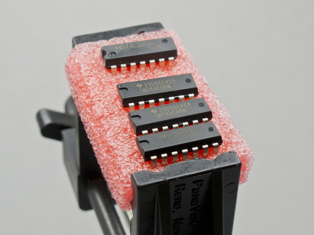
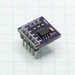
The chips up there are SN74HC00N “Quadruple 2-Input Positive NAND Gates”, from Texas Instruments (datasheet here). Translated, that means there are four NAND gates on that chip, with each gate having an A and a B input, just like our description above. (Coincidentally, the “23” part of the marking above the part number means the chip was manufactured in March-2002, a few months before I wound up buying it). The chip at the very top though, is an “HD74LS00P”, which is manufactured by Renesas — pretty much exactly the same chip from a different manufacturer.
Notice though, that between the two companies part numbers, the “74” and the “00” are the same. If you’ve ever heard the phrase, “Seventy-Four-Hundred Series Logic”, that’s where it comes from. The “00” is the designation for a NAND gate chip. The heiroglyphics associated with 74xx series logic chips is described here in far better detail than I have any desire to go into.
Testing Simple Digital Logic Circuits
Enough already, let’s stick something into a breadboard. We’ll just go down the list and prove each truth table, using the discrete logic chip, and some blinky lights to show the output state.
The chips I’m using are…
- SN74HC00 – QUAD NAND
- SN74HC02 – QUAD NOR
- SN74HC04 – HEX NOT
- SN74HC08 – QUAD AND
- SN74HC86 – QUAD XOR
- HD74LS32 – QUAD OR
If you look at the datasheets for these chips, you’ll see that all of them are limited to a maximum Vcc of 6V, so we can’t just hook up any ol’ voltage source and go to town. I’m using the 5V output on my Arduino and soldered the LED’s to some perfboard so that it would look the same from one picture to the next, but you can use a 9V battery with an LM7805 voltage regulator just as easily. No microcontroller is necessary.
The red LEDs represent the inputs of the truth table, and the green LEDs represent the outputs. I haven’t drawn up any schematics for these to include, because there’s nothing to it really, just connect the input pins to either +5V or GND to comprise the four states the inputs can be combined in (or two states in the case of the NOT gate) and pipe the output to the LEDs, with at least a 150Ω current limiting resistors for each LED (5V – 2Vf = 3V / .020Amax = 150Ω).
[masterslider id=26]
Proof of the XNOR gate truth table…
Wellllllll… turns out I don’t have an XNOR chip. Not to worry though, because NAND and NOR gates are magical: you can build any of the other gates using just those two chip types alone — and being creative with how you combine the inputs. In order to create an XNOR gate out of NOR gates, you would do the following…
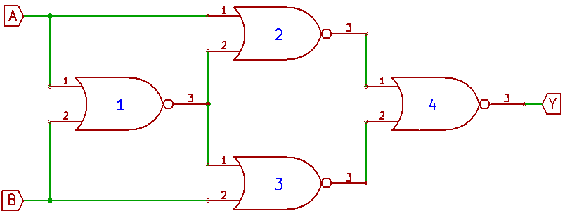
If you have the patience for it, you can generate a truth table for each of the four possible input states…
| INPUT A | INPUT B | NOR GATE 1 | NOR GATE 2 | NOR GATE 3 | NOR GATE 4 | ||||||||
|---|---|---|---|---|---|---|---|---|---|---|---|---|---|
| A | B | PIN 1 | PIN 2 | PIN 3 | PIN 1 | PIN 2 | PIN 3 | PIN 1 | PIN 2 | PIN 3 | PIN 1 | PIN 2 | PIN 3 |
| LOW | LOW | LOW | LOW | HIGH | LOW | HIGH | LOW | HIGH | LOW | LOW | LOW | LOW | HIGH |
| LOW | HIGH | LOW | HIGH | LOW | LOW | LOW | HIGH | LOW | HIGH | LOW | HIGH | LOW | LOW |
| HIGH | LOW | HIGH | LOW | LOW | HIGH | LOW | LOW | LOW | LOW | HIGH | LOW | HIGH | LOW |
| HIGH | HIGH | HIGH | HIGH | LOW | HIGH | LOW | LOW | LOW | HIGH | LOW | LOW | LOW | HIGH |
Measuring Voltage and Current in Digital Logic Circuits
First, let’s look at the pin voltage for each A-B configuration, and measure how much current is drawn by the chip in general for during each input config. For the purposes of the measurement, I’m going to use the XNOR configuration from above, and eliminate all extraneous stuff except for one LED with a current limiting resistor, to give it something to drive.
| INPUT A | INPUT B | CURRENT | NOR GATE 1 | NOR GATE 2 | NOR GATE 3 | NOR GATE 4 | ||||||||
|---|---|---|---|---|---|---|---|---|---|---|---|---|---|---|
| A | B | mA | PIN 1 | PIN 2 | PIN 3 | PIN 1 | PIN 2 | PIN 3 | PIN 1 | PIN 2 | PIN 3 | PIN 1 | PIN 2 | PIN 3 |
| LOW | LOW | 15.74 | 0.00 | 0.00 | 4.87 | 0.00 | 4.87 | 0.00 | 4.87 | 0.00 | 0.00 | 0.00 | 0.00 | 4.29 |
| LOW | HIGH | 0.00 | 0.00 | 5.04 | 0.00 | 0.00 | 0.00 | 5.04 | 0.00 | 5.04 | 0.00 | 5.04 | 0.00 | 0.00 |
| HIGH | LOW | 0.00 | 5.04 | 0.00 | 0.00 | 5.04 | 0.00 | 0.00 | 0.00 | 0.00 | 5.04 | 0.00 | 5.04 | 0.00 |
| HIGH | HIGH | 15.26 | 4.34 | 4.34 | 0.00 | 4.34 | 0.00 | 0.00 | 0.00 | 4.34 | 0.00 | 0.00 | 0.00 | 4.24 |
If you were to overlay that with the logic table above, you’d see that the pin voltages match what their predicted state would be. Now the voltage moves around between 5 and 4 a bit, but I’m using a cheap ST Micro voltage regulator, and the datasheet for the NOR gates has specs at 4.5V and 6V and the results we’re seeing with 5V are falling generally in line.
It’s also interesting to note that when the LED is off, there is still voltage on the pins during the A:B and A:B configurations. That raises the question of “how can there be voltage throughout the various pins, but the chip draws 0 current?” Well, in actuality, the chip is drawing current, but my multimeters don’t have the ability to accurately measure that low. This chip is a “74HC” model, meaning the internals of the chip are actually itty-bitty mosfets that have extremely high input impedance, so you’ll push voltage up against it, but no current. (There is excellent supplemental information about that on the AllAboutCircuits page on CMOS Logic Gates.) When the chip is drawing current, it’s only directing it to the LED, that’s all. So when you have A:B or A:B, you get around 14mA current feeding the LED, but in the other states, the power consumption is remarkably low. Unfortunately I don’t have enough multimeters to measure everything at once, but I measured the voltage and current at “A” in the A:B state, while also measuring the current draw at the Vcc pin: the voltage was 4.34V with 0mA current measured at pin 2 (“A”), while Vcc stayed at 15.26mA.
Next, what constitute high and LOW levels for this particular chip. The datasheet says…
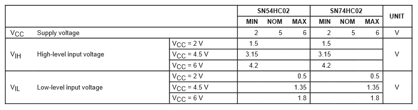
We’ve been using 5(ish) volts, so we’re somewhere between the 4.5V and 6V Vcc ranges for High-level Input Voltage and Low-level Input Voltage. We’ll want to check things in this range then:
- Low range: 1.35V – 1.80V
- High range: 3.15V – 4.20V
To test, I’ve connected the green multimeter in series between the power rail and pin 14 of the chip, so that I’m measuring current draw of the IC. The orange multimeter is measuring voltage at input A, pin 2. What I’m going to do is slowly drop the voltage from 5V down to GND, and see how that affects the current draw on the chip. We want to know if the current just goes ON/OFF when we hit those high and low ranges up there… and what happens in the unspecified middle range between 1.80V and 3.15V.
Specifically this is the XNOR from NOR gates, starting in the A=HIGH / B=LOW state and transitioning to A=LOW / B=LOW.
[masterslider id=27]
What we see is that when when we’re under the specified low threshold of the datasheet, as we should be, we’re drawing within one or two milliamperes of what we were drawing with A connected directly to GND in the table above, 15.74mA vs. 17.4mA .
Now we change things around and we’re going to test A:B transitioning to A:B.
[masterslider id=28]
Again, as we ramp up the voltage to a high output, we see unpredictability become predictability when we arrive within specifications. To really pound the point home, I measured the output pin voltage as well, while measuring Input A going high and Input B = 5V. You would expect to see the output starting low and ending high, but what does it do in between, while the input voltage is slowly ramping up…
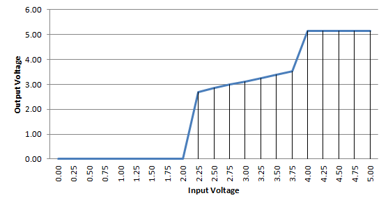
What that tells you is that those middle areas where we’re floating around getting weird current spikes are no place for us to exist. We should be driving the inputs HIGH high or LOW low, not dithering around. After all, these chips aren’t designed for grey area… they’re designed for black and white.
At this point, you could delve deeper into the world of swizzling these things together in various ways, and if pursuing that interests you, I highly recommend the chapter on digital electronics in “Practical Electronics For Inventors“, and doing searches for the topics of …
- Boolean Algebra
- Karnaugh Mapping
- Combinational Logic
- Bubble Pushing